CDB42L55 Cirrus Logic Inc, CDB42L55 Datasheet - Page 17
CDB42L55
Manufacturer Part Number
CDB42L55
Description
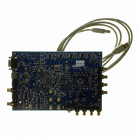
Eval Bd Ultra Low Power Stereo Codec
Manufacturer
Cirrus Logic Inc
Specifications of CDB42L55
Main Purpose
Audio, CODEC
Embedded
Yes, FPGA / CPLD
Utilized Ic / Part
CS42L55
Primary Attributes
2 Stereo Analog Inputs, Stereo Line and Headphone Outputs, S/PDIF Transmitter and Receiver
Secondary Attributes
GUI, USB, RS232, I2C Interfaces, USB or External or Battery Power Supply
Product
Audio Modules
Lead Free Status / RoHS Status
Contains lead / RoHS non-compliant
Lead Free Status / RoHS Status
Contains lead / RoHS non-compliant
Other names
598-1506
CDB-42L55
CDB-42L55


DS773F1
SWITCHING SPECIFICATIONS - SERIAL PORT
Inputs: Logic 0 = GND = AGND, Logic 1 = VL, LRCK, SCLK, SDOUT C
Notes: 17. After powering up the CS42L55, RESET should be held low after the power supplies and clocks are
RESET pin Low Pulse Width
MCLK Frequency
MCLK Duty Cycle
Slave Mode
Input Sample Rate (LRCK)
LRCK Duty Cycle
SCLK Frequency
SCLK Duty Cycle
LRCK Setup Time Before SCLK Rising Edge
SDOUT Setup Time Before SCLK Rising Edge
SDOUT Hold Time After SCLK Rising Edge
SDIN Setup Time Before SCLK Rising Edge
SDIN Hold Time After SCLK Rising Edge
Master Mode
Output Sample Rate (LRCK)
LRCK Duty Cycle
SCLK Frequency
SCLK Duty Cycle
LRCK Time Before SCLK Falling Edge
SDOUT Setup Time Before SCLK Rising Edge
SDOUT Hold Time After SCLK Rising Edge
SDIN Setup Time Before SCLK Rising Edge
SDIN Hold Time After SCLK Rising Edge
SDOUT
LRCK
SCLK
SDIN
Figure 5. Serial Port Timing (Slave Mode)
18. The device will periodically extend the SCLK high time to compensate for the fractional MCLK/SCLK
(Figure
settled. This specification is valid with the recommended capacitor on VDFILT.
ratio.
(Figure
t
ss(LK-SK)
5)
6)
//
//
//
//
//
//
//
t
P
t
Parameters
ss(SDO-SK)
t
ss(SD-SK)
//
//
//
//
MSB
t
MSB
hs(SK-SDO)
t
hs
RATIO[1:0] = ‘01’
//
SCLK = MCLK mode
RATIO[1:0] = ‘11’
All Speed Modes
All Other Modes
SDOUT
LRCK
SCLK
SDIN
(Note 17)
(Note 18)
Figure 6. Serial Port Timing (Master Mode)
LOAD
//
= 15 pF.
t
t
t
t
hm(SK-SDO)
sm(SDO-SK)
t
hs(SK-SDO)
t
Symbol
ss(SDO-SK)
t
t
sm(SD-SK)
sm(LK-SK)
ss(SD-SK)
ss(LK-SK)
t
sm(LK-SK)
1/t
1/t
1/t
t
t
F
F
hm
hs
Pm
Pm
//
s
Ps
s
(See
(See
(See
//
//
//
//
//
//
//
Min
45
45
45
40
20
30
20
20
45
45
33
20
30
20
20
t
“Serial Port Clocking”
“Serial Port Clocking”
“Serial Port Clocking”
Pm
1
-
-
-
-
t
sm(SDO-SK)
t
on page
on page
on page
sm(SD-SK)
//
34)
34)
34)
12.0000
68•F
68•F
Max
//
//
//
t
MSB
55
55
55
55
55
66
±2
MSB
hm(SK-SDO)
CS42L55
-
-
-
-
-
-
-
-
-
-
t
hm
s
s
//
Units
MHz
MHz
kHz
ms
Hz
Hz
Hz
ns
ns
ns
ns
ns
ns
ns
ns
ns
ns
%
%
%
%
%
%
17
Related parts for CDB42L55
Image
Part Number
Description
Manufacturer
Datasheet
Request
R

Part Number:
Description:
Development Kit
Manufacturer:
Cirrus Logic Inc
Datasheet:
Part Number:
Description:
Development Kit
Manufacturer:
Cirrus Logic Inc
Datasheet:


Part Number:
Description:
High-efficiency PFC + Fluorescent Lamp Driver Reference Design
Manufacturer:
Cirrus Logic Inc
Datasheet:
Part Number:
Description:
Development Kit
Manufacturer:
Cirrus Logic Inc
Datasheet:
Part Number:
Description:
Development Kit
Manufacturer:
Cirrus Logic Inc
Datasheet:

Part Number:
Description:
Development Kit
Manufacturer:
Cirrus Logic Inc
Datasheet:
Part Number:
Description:
Development Kit
Manufacturer:
Cirrus Logic Inc
Datasheet:
Part Number:
Description:
Development Kit
Manufacturer:
Cirrus Logic Inc
Datasheet:
Part Number:
Description:
Development Kit
Manufacturer:
Cirrus Logic Inc
Datasheet:

Part Number:
Description:
EVALUATION BOARD FOR CS8427
Manufacturer:
Cirrus Logic Inc
Datasheet:

Part Number:
Description:
BOARD EVAL FOR CS8416 RCVR
Manufacturer:
Cirrus Logic Inc
Datasheet:

Part Number:
Description:
EVALUATION BOARD FOR CS8420
Manufacturer:
Cirrus Logic Inc
Datasheet:

Part Number:
Description:
KIT DEVELOPMENT EP9315 ARM9
Manufacturer:
Cirrus Logic Inc
Datasheet:

Part Number:
Description:
KIT DEVELOPMENT EP9302 ARM9
Manufacturer:
Cirrus Logic Inc
Datasheet: