CDB42L55 Cirrus Logic Inc, CDB42L55 Datasheet - Page 6
CDB42L55
Manufacturer Part Number
CDB42L55
Description
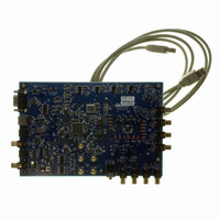
Eval Bd Ultra Low Power Stereo Codec
Manufacturer
Cirrus Logic Inc
Specifications of CDB42L55
Main Purpose
Audio, CODEC
Embedded
Yes, FPGA / CPLD
Utilized Ic / Part
CS42L55
Primary Attributes
2 Stereo Analog Inputs, Stereo Line and Headphone Outputs, S/PDIF Transmitter and Receiver
Secondary Attributes
GUI, USB, RS232, I2C Interfaces, USB or External or Battery Power Supply
Product
Audio Modules
Lead Free Status / RoHS Status
Contains lead / RoHS non-compliant
Lead Free Status / RoHS Status
Contains lead / RoHS non-compliant
Other names
598-1506
CDB-42L55
CDB-42L55


6
LIST OF FIGURES
7. PCB LAYOUT CONSIDERATIONS ..................................................................................................... 68
8. ANALOG VOLUME NON-LINEARITY (DNL & INL) ............................................................................ 69
9. ADC & DAC DIGITAL FILTERS .......................................................................................................... 70
10. PARAMETER DEFINITIONS .............................................................................................................. 71
11. PACKAGE DIMENSIONS .................................................................................................................. 72
12. ORDERING INFORMATION .............................................................................................................. 73
13. REFERENCES .................................................................................................................................... 73
14. REVISION HISTORY .......................................................................................................................... 73
Figure 1.Typical Connection Diagram ....................................................................................................... 10
Figure 2.CMRR Test Configuration ........................................................................................................... 12
Figure 3.HP Output Test Configuration ..................................................................................................... 15
Figure 4.Line Output Test Configuration ................................................................................................... 15
Figure 5.Serial Port Timing (Slave Mode) ................................................................................................. 17
Figure 6.Serial Port Timing (Master Mode) ............................................................................................... 17
Figure 7.I²C Control Port Timing ............................................................................................................... 18
Figure 8.Power Consumption Test Configuration ..................................................................................... 19
Figure 9.Analog Input Signal Flow ............................................................................................................ 23
Figure 10.Stereo Pseudo-Differential Input ............................................................................................... 24
Figure 11.ALC Operation .......................................................................................................................... 25
Figure 12.DSP Engine Signal Flow ........................................................................................................... 26
Figure 13.Analog Output Stage ................................................................................................................. 27
Figure 14.Adaptive Mode 00 ..................................................................................................................... 28
Figure 15.VHPFILT Transitions ................................................................................................................. 30
Figure 16.VHPFILT Hysteresis ................................................................................................................. 30
Figure 17.Class H Power to Load vs. Power from VCP Supply ................................................................ 31
THERMAL CHARACTERISTICS .......................................................................................................... 72
6.30 ALC Release Rate (Address 25h) ................................................................................................ 63
6.31 ALC Threshold (Address 26h) ...................................................................................................... 64
6.32 Noise Gate Control (Address 27h) ............................................................................................... 64
6.33 ALC and Limiter Soft Ramp, Zero Cross Disables (Address 28h) ................................................ 65
6.34 Status (Address 29h) (Read Only) ............................................................................................... 66
6.35 Charge Pump Frequency (Address 2Ah) ..................................................................................... 67
7.1 Power Supply ................................................................................................................................. 68
7.2 Grounding ....................................................................................................................................... 68
7.3 QFN Thermal Pad .......................................................................................................................... 68
6.30.1 ALC Release Rate ............................................................................................................... 63
6.31.1 ALC Maximum Threshold .................................................................................................... 64
6.31.2 ALC Minimum Threshold ..................................................................................................... 64
6.32.1 Noise Gate All Channels ..................................................................................................... 64
6.32.2 Noise Gate Enable .............................................................................................................. 65
6.32.3 Noise Gate Threshold and Boost ........................................................................................ 65
6.32.4 Noise Gate Delay Timing .................................................................................................... 65
6.33.1 ALCx Soft Ramp Disable ..................................................................................................... 65
6.33.2 ALCx Zero Cross Disable .................................................................................................... 65
6.33.3 Limiter Soft Ramp Disable ................................................................................................... 66
6.34.1 HPDETECT Pin Status (Read Only) ................................................................................... 66
6.34.2 Serial Port Clock Error (Read Only) .................................................................................... 66
6.34.3 DSP Engine Overflow (Read Only) ..................................................................................... 66
6.34.4 MIXx Overflow (Read Only) ................................................................................................. 66
6.34.5 ADCx Overflow (Read Only) ............................................................................................... 67
6.35.1 Charge Pump Frequency .................................................................................................... 67
CS42L55
DS773F1
Related parts for CDB42L55
Image
Part Number
Description
Manufacturer
Datasheet
Request
R

Part Number:
Description:
Development Kit
Manufacturer:
Cirrus Logic Inc
Datasheet:
Part Number:
Description:
Development Kit
Manufacturer:
Cirrus Logic Inc
Datasheet:


Part Number:
Description:
High-efficiency PFC + Fluorescent Lamp Driver Reference Design
Manufacturer:
Cirrus Logic Inc
Datasheet:
Part Number:
Description:
Development Kit
Manufacturer:
Cirrus Logic Inc
Datasheet:
Part Number:
Description:
Development Kit
Manufacturer:
Cirrus Logic Inc
Datasheet:

Part Number:
Description:
Development Kit
Manufacturer:
Cirrus Logic Inc
Datasheet:
Part Number:
Description:
Development Kit
Manufacturer:
Cirrus Logic Inc
Datasheet:
Part Number:
Description:
Development Kit
Manufacturer:
Cirrus Logic Inc
Datasheet:
Part Number:
Description:
Development Kit
Manufacturer:
Cirrus Logic Inc
Datasheet:

Part Number:
Description:
EVALUATION BOARD FOR CS8427
Manufacturer:
Cirrus Logic Inc
Datasheet:

Part Number:
Description:
BOARD EVAL FOR CS8416 RCVR
Manufacturer:
Cirrus Logic Inc
Datasheet:

Part Number:
Description:
EVALUATION BOARD FOR CS8420
Manufacturer:
Cirrus Logic Inc
Datasheet:

Part Number:
Description:
KIT DEVELOPMENT EP9315 ARM9
Manufacturer:
Cirrus Logic Inc
Datasheet:

Part Number:
Description:
KIT DEVELOPMENT EP9302 ARM9
Manufacturer:
Cirrus Logic Inc
Datasheet: