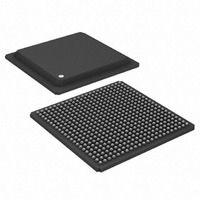
ADSP-TS101SAB2-000 Analog Devices Inc, ADSP-TS101SAB2-000 Datasheet - Page 10

ADSP-TS101SAB2-000
Manufacturer Part Number
ADSP-TS101SAB2-000
Description
IC,DSP,32-BIT,BGA,484PIN,PLASTIC
Manufacturer
Analog Devices Inc
Series
TigerSHARC®r
Type
Fixed/Floating Pointr
Datasheet
1.ADSP-TS101SAB1-000.pdf
(48 pages)
Specifications of ADSP-TS101SAB2-000
Rohs Status
RoHS non-compliant
Interface
Host Interface, Link Port, Multi-Processor
Clock Rate
250MHz
Non-volatile Memory
External
On-chip Ram
768kB
Voltage - I/o
3.30V
Voltage - Core
1.20V
Operating Temperature
-40°C ~ 85°C
Mounting Type
Surface Mount
Package / Case
484-BGA
Package
484BGA
Numeric And Arithmetic Format
Fixed-Point|Floating-Point
Maximum Speed
250 MHz
Ram Size
768 KB
Device Million Instructions Per Second
250 MIPS
Lead Free Status / RoHS Status
Other names
ADSP-TS101SAB2000
Available stocks
Company
Part Number
Manufacturer
Quantity
Price
Company:
Part Number:
ADSP-TS101SAB2-000
Manufacturer:
MINI
Quantity:
1 400
Company:
Part Number:
ADSP-TS101SAB2-000
Manufacturer:
Analog Devices Inc
Quantity:
10 000
ADSP-TS101S
Connecting SCLK and LCLK to the same clock source is a
requirement for the device. Using an integer clock multiplica-
tion value provides predictable cycle-by-cycle operation, a
requirement of fault-tolerant systems and some multiprocessing
systems.
Noninteger values are completely functional and acceptable for
applications that do not require predictable cycle-by-cycle
operation.
OUTPUT PIN DRIVE STRENGTH CONTROL
Pins CONTROLIMP2–0 and DS2–0 work together to control
the output drive strength of two groups of pins, the
Address/Data/Control pin group and the Link pin group.
CONTROLIMP2–0 independently configures the two pin
groups to the maximum drive strength or to a digitally con-
trolled drive strength that is selectable by the DS2–0 pins (see
Table 13 on Page
selected for a pin group, the DS2–0 pins determine one of eight
strength levels for that group (see
drive strength selected varies the slew rate of the driver. Drive
strength 0 (DS2–0 = 000) is the weakest and slowest slew rate.
Drive strength 7 (DS2–0 = 111) is the strongest and fastest slew
rate.
The stronger drive strengths are useful for high frequency
switching while the lower strengths may allow use of a relaxed
design methodology. The strongest drive strengths have a larger
di/dt and thus require more attention to signal integrity issues
such a ringing, reflections and coupling. Also, a larger di/dt can
increase external supply rail noise, which impacts power supply
and power distribution design.
The drive strengths for the EMU, CPA, and DPA pins are not
controllable and are fixed to the maximum level.
For drive strength calculation, see
Page
POWER SUPPLIES
The ADSP-TS101S has separate power supply connections for
internal logic (V
(V
supplies must meet the 1.2 V requirement. The I/O buffer
(V
The analog supply (V
produce a stable clock, systems must provide a clean power sup-
ply to power input V
bypassing the V
The required power-on sequence for the DSP is to provide V
(and V
DD_IO
DD_IO
ates CCLK, which is phase-locked. The LCLKRAT pins
define the clock multiplication of LCLK to CCLK (see
Table
software programmable divisor. RESET must be asserted
until LCLK is stable and within specification for at least
2 ms. This applies to power-up as well as any dynamic
modification of LCLK after power-up. Dynamic modifica-
tion may include LCLK going out of specification as long as
RESET is asserted.
32.
DD_A
) power supply. The internal (V
) supply must meet the 3.3 V requirement.
4). The link port clock is generated from CCLK via a
) before V
DD_A
DD
18). If the digitally controlled drive strength is
), analog circuits (V
supply.
DD_A
DD_IO
DD_A
. Designs must pay critical attention to
) powers the clock generator PLLs. To
.
Table 14 on Page
Output Drive Currents on
DD_A
DD
) and analog (V
), and I/O buffer
18). The
Rev. C | Page 10 of 48 | May 2009
DD_A
DD
)
FILTERING REFERENCE VOLTAGE AND CLOCKS
Figure 6
LCLK_N. This circuit provides the reference voltage for the
switching voltage, system clock, and local clock references.
DEVELOPMENT TOOLS
The ADSP-TS101S is supported with a complete set of
CROSSCORE
including Analog Devices emulators and VisualDSP++
opment environment. The same emulator hardware that
supports other TigerSHARC processors also fully emulates the
ADSP-TS101S.
The VisualDSP++ project management environment lets pro-
grammers develop and debug an application. This environment
includes an easy to use assembler (which is based on an alge-
braic syntax), an archiver (librarian/library builder), a linker, a
loader, a cycle-accurate instruction-level simulator, a C/C++
compiler, and a C/C++ run-time library that includes DSP and
mathematical functions. A key point for these tools is C/C++
code efficiency. The compiler has been developed for efficient
translation of C/C++ code to DSP assembly. The DSP has archi-
tectural features that improve the efficiency of compiled C/C++
code.
The VisualDSP++ debugger has a number of important fea-
tures. Data visualization is enhanced by a plotting package that
offers a significant level of flexibility. This graphical representa-
tion of user data enables the programmer to quickly determine
the performance of an algorithm. As algorithms grow in com-
plexity, this capability can have increasing significance on the
designer’s development schedule, increasing productivity. Sta-
tistical profiling enables the programmer to nonintrusively poll
the processor as it is running the program. This feature, unique
to VisualDSP++, enables the software developer to passively
gather important code execution metrics without interrupting
the real-time characteristics of the program. Essentially, the
developer can identify bottlenecks in software quickly and
efficiently. By using the profiler, the programmer can focus on
those areas in the program that impact performance and take
corrective action.
†
‡
CROSSCORE is a registered trademark of Analog Devices, Inc.
VisualDSP++ is a registered trademark of Analog Devices, Inc.
R1: 2k
R2: 1.67k
C1: 1 F CAPACITOR (SMD)
C2: 1nF CAPACITOR (HF SMD) PLACED CLOSE TO DSP’S PINS
V
shows a possible circuit for filtering V
DD_IO
SERIES RESISTOR
®†
Figure 6. V
SERIES RESISTOR
software and hardware development tools,
R1
R2
REF
, SCLK_N, and LCLK_N Filter
C1
V
SS
C2
REF
, SCLK_N, and
SCLK_N
LCLK_N
V
REF
®‡
devel-


