ADSP-TS101SAB2-000 Analog Devices Inc, ADSP-TS101SAB2-000 Datasheet - Page 27
ADSP-TS101SAB2-000
Manufacturer Part Number
ADSP-TS101SAB2-000
Description
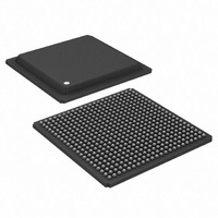
IC,DSP,32-BIT,BGA,484PIN,PLASTIC
Manufacturer
Analog Devices Inc
Series
TigerSHARC®r
Type
Fixed/Floating Pointr
Datasheet
1.ADSP-TS101SAB1-000.pdf
(48 pages)
Specifications of ADSP-TS101SAB2-000
Rohs Status
RoHS non-compliant
Interface
Host Interface, Link Port, Multi-Processor
Clock Rate
250MHz
Non-volatile Memory
External
On-chip Ram
768kB
Voltage - I/o
3.30V
Voltage - Core
1.20V
Operating Temperature
-40°C ~ 85°C
Mounting Type
Surface Mount
Package / Case
484-BGA
Package
484BGA
Numeric And Arithmetic Format
Fixed-Point|Floating-Point
Maximum Speed
250 MHz
Ram Size
768 KB
Device Million Instructions Per Second
250 MIPS
Lead Free Status / RoHS Status
Other names
ADSP-TS101SAB2000
Available stocks
Company
Part Number
Manufacturer
Quantity
Price
Company:

Part Number:
ADSP-TS101SAB2-000
Manufacturer:
MINI
Quantity:
1 400
Company:
Part Number:
ADSP-TS101SAB2-000
Manufacturer:
Analog Devices Inc
Quantity:
10 000


Table 28. AC Signal Specifications (for 16.7 ns <SCLK <25 ns) (All values in this table are in nanoseconds) (Continued)
1
2
3
4
5
6
7
8
9
10
11
12
Name
RESET
TMS
TDI
TDO
TRST
BM
EMU
JTAG_SYS_IN
JTAG_SYS_OUT
ID2–0
CONTROLIMP2–0
DS2–0
LCLKRAT2–0
SCLKFREQ
The output valid (max) value in this column applies for the standard 30 pF capacitive load used in testing. To see how output valid varies with capacitive loading, see
The external port protocols employ bus IDLE cycles for bus mastership transitions as well as slave address boundary crossings to avoid any potential bus contention. The
CPA and DPA pins are open drains and have 0.5 k internal pull-ups.
These input pins have Schmitt triggers and therefore do not need to be synchronized to a clock reference. These synchronous specifications only apply for recognition in the
This pin is a strap option. During reset, an internal resistor pulls the pin low.
For input specifications, see
For additional requirement details, see
TCK_FE indicates TCK falling edge.
These pins may change only during reset; recommend connecting it to V
Reference clock depends on function.
System inputs are: IRQ3–0, BMS, LCLKRAT2–0, SCLKFREQ, BM, TMR0E, FLAG3–0, ID2–0, BRST, WRH, WRL, RD, MSSD, SDCKE, SDWE, CAS, RAS, ADDR31–0,
System outputs are: BMS, BM, BUSLOCK, TMR0E, FLAG3–0, FLYBY, IOEN, MSH, BRST, WRH, WRL, RD, MS1–0, HDQM, LDQM, MSSD, SDCKE, SDWE, CAS, RAS,
on Page
apparent driver overlap, due to output disables being larger than output enables, is not actual.
current clock reference cycle.
DATA63–0, DPA, CPA, HBG, BOFF, HBR, ACK, BR7–0, L0CLKIN, L0DAT7–0, L1CLKIN, L1DAT7–0, L2CLKIN, L2DAT7–0, L2DIR, L3CLKIN, L3DAT7–0, DS2–0,
CONTROLIMP2–0, RESET, DMAR3–0.
ADDR31–0, DATA63–0, DPA, CPA, HBG, ACK, BR7–0, L0CLKOUT, L0DAT7–0, L0DIR, L1CLKOUT, L1DAT7–0, L1DIR, L2CLKOUT, L2DAT7–0, L2DIR, L3CLKOUT,
L3DAT7–0, L3DIR, EMU.
5
4
4
10
4, 7, 9
9
4, 7
9
36.
9
9
11
12
9
Table
Description
Global Reset
Test Mode Select (JTAG)
Test Data Input (JTAG)
Test Data Output (JTAG)
Test Reset (JTAG)
Bus Master Debug Aid Only
Emulation
System Input
System Output
Chip ID—Must Be Constant
Static Pins—Must Be Constant
Static Pins—Must Be Constant
Static Pins—Must Be Constant
Static Pins—Must Be Constant
21.
Reset and Booting on Page
Rev. C | Page 27 of 48 | May 2009
9.
DD_IO
/V
SS
.
1.5
1.5
1.5
1.0
1.0
11.0
6.0
5.5
4.2
16.0
1.0
0.8
1.0
ADSP-TS101S
5.0
5.0
TCK
TCK_FE
SCLK
TCK
TCK
SCLK
TCK or LCLK
TCK
TCK_FE
Figure 40
8
8
Related parts for ADSP-TS101SAB2-000
Image
Part Number
Description
Manufacturer
Datasheet
Request
R

Part Number:
Description:
±1.7g Dual-Axis IMEMS Accelerometer Evaluation Board
Manufacturer:
Analog Devices Inc
Datasheet:

Part Number:
Description:
Inertial Sensor Evaluation System
Manufacturer:
Analog Devices Inc
Datasheet:
Part Number:
Description:
Manufacturer:
Analog Devices Inc
Datasheet:
Part Number:
Description:
Manufacturer:
Analog Devices Inc
Datasheet:
Part Number:
Description:
Manufacturer:
Analog Devices Inc
Datasheet:
Part Number:
Description:
Manufacturer:
Analog Devices Inc
Datasheet:
Part Number:
Description:
Manufacturer:
Analog Devices Inc
Datasheet:
Part Number:
Description:
Manufacturer:
Analog Devices Inc
Datasheet:
Part Number:
Description:
Manufacturer:
Analog Devices Inc
Datasheet:
Part Number:
Description:
Manufacturer:
Analog Devices Inc
Datasheet:
Part Number:
Description:
Manufacturer:
Analog Devices Inc
Datasheet:
Part Number:
Description:
Manufacturer:
Analog Devices Inc
Datasheet:
Part Number:
Description:
Manufacturer:
Analog Devices Inc
Datasheet: