ADSP-TS101SAB2-000 Analog Devices Inc, ADSP-TS101SAB2-000 Datasheet - Page 29
ADSP-TS101SAB2-000
Manufacturer Part Number
ADSP-TS101SAB2-000
Description
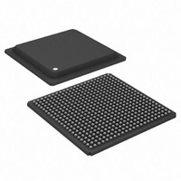
IC,DSP,32-BIT,BGA,484PIN,PLASTIC
Manufacturer
Analog Devices Inc
Series
TigerSHARC®r
Type
Fixed/Floating Pointr
Datasheet
1.ADSP-TS101SAB1-000.pdf
(48 pages)
Specifications of ADSP-TS101SAB2-000
Rohs Status
RoHS non-compliant
Interface
Host Interface, Link Port, Multi-Processor
Clock Rate
250MHz
Non-volatile Memory
External
On-chip Ram
768kB
Voltage - I/o
3.30V
Voltage - Core
1.20V
Operating Temperature
-40°C ~ 85°C
Mounting Type
Surface Mount
Package / Case
484-BGA
Package
484BGA
Numeric And Arithmetic Format
Fixed-Point|Floating-Point
Maximum Speed
250 MHz
Ram Size
768 KB
Device Million Instructions Per Second
250 MIPS
Lead Free Status / RoHS Status
Other names
ADSP-TS101SAB2000
Available stocks
Company
Part Number
Manufacturer
Quantity
Price
Company:

Part Number:
ADSP-TS101SAB2-000
Manufacturer:
MINI
Quantity:
1 400
Company:
Part Number:
ADSP-TS101SAB2-000
Manufacturer:
Analog Devices Inc
Quantity:
10 000


Link Ports Data Transfer and Token Switch Timing
Table
Figure
tions for the link ports data transfer and token switch.
Table 29. Link Ports—Transmit
1
2
3
4
5
Parameter
Timing Requirements
t
t
t
t
Switching Characteristics
t
t
t
t
t
t
t
t
t
t
t
t
t
The formula for this parameter applies when LR is 2.
The formula for this parameter applies when LR is 3, 4, or 8.
LxCLKIN shows the connectivity pulse with each of the three possible transitions to “Acknowledge.” After a connectivity pulse low minimum, LxCLKIN may [1] return high
The Link clock Ratio (LR) is 2, 3, 4, or 8 as set by the SPD bits in the LCTLx register. The maximum LxCLK is 125 MHz. LR = 2 may not be used when CCLK 250 MHz.
This specification applies to the last data byte or the “Dummy” byte that follows the verification byte if enabled. For more information, see the ADSP-TS101 TigerSHARC
CONNS
CONNS
CONNIW
ACKS
L
L
L
L
L
DIRS
DIRH
DOS
DOH
DOS
DOH
LDOE
LDOD
and remain high for “Acknowledge,” [2] return high and subsequently go low (meeting t
Processor Hardware Reference.
X
X
X
X
X
CLK_T
CLKH_T
CLKH_T
CLKL_T
CLKL_T
1
2
1
2
5
31,
1
2
X
18,
3
4
X
X
X
X
1
2
1
2
LxCLKOUT
LxDAT7–0
Table
Figure
LxCLKIN
LxDIR
32,
19, and
Table
Connectivity Pulse Setup
Connectivity Pulse Setup
Connectivity Pulse Input Width
Acknowledge Setup
Transmit Link Clock Period
Transmit Link Clock Width High
Transmit Link Clock Width High
Transmit Link Clock Width Low
Transmit Link Clock Width Low
LxDIR Transmit Setup
LxDIR Transmit Hold
LxDAT7–0 Output Setup
LxDAT7–0 Output Hold
LxDAT7–0 Output Setup
LxDAT7–0 Output Hold
LxDAT7–0 Output Enable
LxDAT7–0 Output Disable
t
Figure 20
33, and
DIRS
t
LDOE
0
t
Table 34
LxCLKH_Tx
provide the timing specifica-
1
2
t
with
LxCLK_Tx
3
Figure
t
4
LxCLKL_Tx
Rev. C | Page 29 of 48 | May 2009
Figure 17. Link Ports—Transmit
17,
5
t
6
CONNIW
t
DOS
7
t
DOH
8
t
CONNS
ACKS
) for “Not Acknowledge,” or [3] remain low for “Not Acknowledge.”
9
t
DOS
Min
2
8
t
0.5
0.9
0.33
0.4
0.33
0.4
0.5
0.5
0.25
0.25
Greater of 0.8 or 0.17
Greater of 0.8 or 0.17
1
1
10
L
X
CLK_T
t
t
ACKS
CCLK
t
t
LR
t
t
t
t
DOH
11
L
L
L
L
L
X
t
t
t
t
X
X
X
X
X
+ 1
L
L
L
L
CLK_T
CLK_T
CLK_T
CLK_T
CLK_T
X
X
X
X
+ 3.5
CLK_T
CLK_T
CLK_T
CLK_T
t
12
CCLK
X
X
X
X
X
X
X
X
X
– 1
– 1
13
14
t
t
L
L
15
X
X
CLK_T
CLK_T
t
LDOD
t
X
X
DIRH
– 1
– 1
Max
1.1
0.66
0.6
0.66
0.6
2
2
ADSP-TS101S
t
t
L
L
X
X
LR
t
t
CLK_T
CLK_T
L
L
t
t
X
X
L
CLK_T
L
CLK_T
X
X
CLK_T
CLK_T
X
X
t
CCLK
X
X
X
X
Unit
ns
ns
ns
ns
ns
ns
ns
ns
ns
ns
ns
ns
ns
ns
ns
ns
ns
Related parts for ADSP-TS101SAB2-000
Image
Part Number
Description
Manufacturer
Datasheet
Request
R

Part Number:
Description:
±1.7g Dual-Axis IMEMS Accelerometer Evaluation Board
Manufacturer:
Analog Devices Inc
Datasheet:

Part Number:
Description:
Inertial Sensor Evaluation System
Manufacturer:
Analog Devices Inc
Datasheet:
Part Number:
Description:
Manufacturer:
Analog Devices Inc
Datasheet:
Part Number:
Description:
Manufacturer:
Analog Devices Inc
Datasheet:
Part Number:
Description:
Manufacturer:
Analog Devices Inc
Datasheet:
Part Number:
Description:
Manufacturer:
Analog Devices Inc
Datasheet:
Part Number:
Description:
Manufacturer:
Analog Devices Inc
Datasheet:
Part Number:
Description:
Manufacturer:
Analog Devices Inc
Datasheet:
Part Number:
Description:
Manufacturer:
Analog Devices Inc
Datasheet:
Part Number:
Description:
Manufacturer:
Analog Devices Inc
Datasheet:
Part Number:
Description:
Manufacturer:
Analog Devices Inc
Datasheet:
Part Number:
Description:
Manufacturer:
Analog Devices Inc
Datasheet:
Part Number:
Description:
Manufacturer:
Analog Devices Inc
Datasheet: