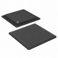
ADSP-TS101SAB2-000 Analog Devices Inc, ADSP-TS101SAB2-000 Datasheet - Page 12

ADSP-TS101SAB2-000
Manufacturer Part Number
ADSP-TS101SAB2-000
Description
IC,DSP,32-BIT,BGA,484PIN,PLASTIC
Manufacturer
Analog Devices Inc
Series
TigerSHARC®r
Type
Fixed/Floating Pointr
Datasheet
1.ADSP-TS101SAB1-000.pdf
(48 pages)
Specifications of ADSP-TS101SAB2-000
Rohs Status
RoHS non-compliant
Interface
Host Interface, Link Port, Multi-Processor
Clock Rate
250MHz
Non-volatile Memory
External
On-chip Ram
768kB
Voltage - I/o
3.30V
Voltage - Core
1.20V
Operating Temperature
-40°C ~ 85°C
Mounting Type
Surface Mount
Package / Case
484-BGA
Package
484BGA
Numeric And Arithmetic Format
Fixed-Point|Floating-Point
Maximum Speed
250 MHz
Ram Size
768 KB
Device Million Instructions Per Second
250 MIPS
Lead Free Status / RoHS Status
Other names
ADSP-TS101SAB2000
Available stocks
Company
Part Number
Manufacturer
Quantity
Price
Company:
Part Number:
ADSP-TS101SAB2-000
Manufacturer:
MINI
Quantity:
1 400
Company:
Part Number:
ADSP-TS101SAB2-000
Manufacturer:
Analog Devices Inc
Quantity:
10 000
ADSP-TS101S
PIN FUNCTION DESCRIPTIONS
While most of the ADSP-TS101S processor’s input pins are nor-
mally synchronous—tied to a specific clock—a few are
asynchronous. For these asynchronous signals, an on-chip syn-
chronization circuit prevents metastability problems. The
synchronous ac specification for asynchronous signals is used
only when predictable cycle-by-cycle behavior is required.
All inputs are sampled by a clock reference, therefore input
specifications (asynchronous minimum pulse widths or syn-
chronous input setup and hold) must be met to guarantee
recognition.
Table 3. Pin Definitions—Clocks and Reset
1
2
3
Table 4. LCLK Ratio
Signal
LCLK_N
LCLK_P
LCLKRAT2–0
SCLK_N
SCLK_P
SCLKFREQ
RESET
Type column symbols: A = asynchronous; G = ground; I = input; O = output; o/d = open drain output; P = power supply;
pd = internal pull-down approximately 100 k
Term (for termination) column symbols: epd = external pull-down approximately 10 k
to V
LCLKRAT2–0
000 (default)
001
010
011
100
101
110
111
The internal pull-down may not be sufficient. A stronger pull-down may be necessary.
See
The internal pull-up may not be sufficient. A stronger pull-up may be necessary.
Electrical Characteristics on Page 20
DD-IO
, nc = not connected; au = always used.
3
1
Type
I
I
I (pd
I
I
I (pu
I/A
2
2
)
)
for maximum and minimum current consumption for pull-up and pull-down resistances.
Term
au
au
au
au
au
au
au
Ratio
2
2.5
3
3.5
4
5
6
Reserved
Description
Local Clock Reference. Connect this pin to V
Local Clock Input. DSP clock input. The instruction cycle rate = n LCLK, where n is user-
programmable to 2, 2.5, 3, 3.5, 4, 5, or 6.
LCLK Ratio. The DSP’s core clock (instruction cycle rate) = n LCLK, where n is user-program-
mable to 2, 2.5, 3, 3.5, 4, 5, or 6 as shown in
the DSP is powered.
System Clock Reference. Connect this pin to V
System Clock Input. The DSP’s system input clock for cluster bus. This pin must be connected
to the same clock source as LCLK_P.
SCLK Frequency. SCLKFREQ = 1 is required. The SCLKFREQ pin must have a constant value while
the DSP is powered.
Reset. Sets the DSP to a known state and causes program to be in idle state. RESET must be
asserted at specified time according to the type of reset operation. For details, see
Booting on Page
; pu = internal pull-up approximately 100 k
Rev. C | Page 12 of 48 | May 2009
9.
PIN STATES AT RESET
The output pins can be three-stated during normal operation.
The DSP three-states all outputs during reset, allowing these
pins to get to their internal pull-up or pull-down state. Some
output pins (control signals) have a pull-up or pull-down that
maintains a known value during transitions between different
drivers.
PIN DEFINITIONS
The Type column in the following pin definitions tables
describes the pin type, when the pin is used in the system. The
Term (for termination) column describes the pin termination
type if the pin is not used by the system. Note that some pins are
always used (indicated with au symbol).
For more information, see Clock Domains on Page 9.
For more information, see Clock Domains on Page 9.
Table
REF
to V
REF
; T = three-state
as shown in
4. These pins must have a constant value while
SS
as shown in
; epu = external pull-up approximately 10 k
Figure
Figure
6.
6.
Reset and


