ADSP-TS101SAB2-000 Analog Devices Inc, ADSP-TS101SAB2-000 Datasheet - Page 9
ADSP-TS101SAB2-000
Manufacturer Part Number
ADSP-TS101SAB2-000
Description
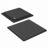
IC,DSP,32-BIT,BGA,484PIN,PLASTIC
Manufacturer
Analog Devices Inc
Series
TigerSHARC®r
Type
Fixed/Floating Pointr
Datasheet
1.ADSP-TS101SAB1-000.pdf
(48 pages)
Specifications of ADSP-TS101SAB2-000
Rohs Status
RoHS non-compliant
Interface
Host Interface, Link Port, Multi-Processor
Clock Rate
250MHz
Non-volatile Memory
External
On-chip Ram
768kB
Voltage - I/o
3.30V
Voltage - Core
1.20V
Operating Temperature
-40°C ~ 85°C
Mounting Type
Surface Mount
Package / Case
484-BGA
Package
484BGA
Numeric And Arithmetic Format
Fixed-Point|Floating-Point
Maximum Speed
250 MHz
Ram Size
768 KB
Device Million Instructions Per Second
250 MIPS
Lead Free Status / RoHS Status
Other names
ADSP-TS101SAB2000
Available stocks
Company
Part Number
Manufacturer
Quantity
Price
Company:

Part Number:
ADSP-TS101SAB2-000
Manufacturer:
MINI
Quantity:
1 400
Company:
Part Number:
ADSP-TS101SAB2-000
Manufacturer:
Analog Devices Inc
Quantity:
10 000


LINK PORTS
The DSP’s four link ports provide additional 8-bit bidirectional
I/O capability. With the ability to operate at a double data rate—
latching data on both the rising and falling edges of the clock—
running at 125 MHz, each link port can support up to
250M bytes per second, for a combined maximum throughput
of 1G bytes per second.
The link ports provide an optional communications channel
that is useful in multiprocessor systems for implementing point-
to-point interprocessor communications. Applications can also
use the link ports for booting.
Each link port has its own double-buffered input and output
registers. The DSP’s core can write directly to a link port’s trans-
mit register and read from a receive register, or the DMA
controller can perform DMA transfers through eight (four
transmit and four receive) dedicated link port DMA channels.
Each link port has three signals that control its operation.
LxCLKOUT and LxCLKIN implement clock/acknowledge
handshaking. LxDIR indicates the direction of transfer and is
used only when buffering the LxDAT signals. An example appli-
cation would be using differential low-swing buffers for long
twisted-pair wires. LxDAT provides the 8-bit data bus
input/output.
Applications can program separate error detection mechanisms
for transmit and receive operations (applications can use the
checksum mechanism to implement consecutive link port
transfers), the size of data packets, and the speed at which bytes
are transmitted.
Under certain conditions, the link port receiver can initiate a
token switch to reverse the direction of transfer; the transmitter
becomes the receiver and vice versa.
TIMER AND GENERAL-PURPOSE I/O
The ADSP-TS101S has a timer pin (TMR0E) that generates out-
put when a programmed timer counter has expired. Also, the
DSP has four programmable general-purpose I/O pins
(FLAG3–0) that can function as either single-bit input or out-
put. As outputs, these pins can signal peripheral devices; as
inputs, they can provide the test for conditional branching.
RESET AND BOOTING
The ADSP-TS101S has two levels of reset (see reset specifica-
tions
The DSP can be reset internally (core reset) by setting the
SWRST bit in SQCTL. The core is reset, but not the external
port or I/O.
• Power-up reset—after power-up of the system, and strap
• Normal reset—for any resets following the power-up reset
options are stable, the RESET pin must be asserted (low).
sequence, the RESET pin must be asserted.
Page
24):
Rev. C | Page 9 of 48 | May 2009
After reset, the ADSP-TS101S has four boot options for begin-
ning operation:
The ADSP-TS101S core always exits from reset in the idle state
and waits for an interrupt. Some of the interrupts in the inter-
rupt vector table are initialized and enabled after reset.
LOW POWER OPERATION
The ADSP-TS101S can enter a low power sleep mode in which
its core does not execute instructions, reducing power con-
sumption to a minimum. The ADSP-TS101S exits sleep mode
when it senses a falling edge on any of its IRQ3–0 interrupt
inputs. The interrupt, if enabled, causes the ADSP-TS101S to
execute the corresponding interrupt service routine. This fea-
ture is useful for systems that require a low power standby
mode.
CLOCK DOMAINS
As shown in
SCLK (system clock) and LCLK (local clock).
These inputs drive its two major clock domains:
• Boot from EPROM. The DSP defaults to EPROM booting
• Boot by an external master (host or another ADSP-
• Boot by link port. All four receive link DMA channels are
• No boot—Start running from an external memory. Using
• SCLK (system clock). Provides clock input for the external
• LCLK (local clock). Provides clock input to the internal
LCLKRATx
when the BMS pin strap option is set low. See
Function Descriptions on Page
TS101S). Any master on the cluster bus can boot the
ADSP-TS101S through writes to its internal memory or
through autoDMA.
initialized after reset to transfer a 256-word block to inter-
nal memory address 0 to 255, and to issue an interrupt at
the end of the block (similar to EP DMA). The correspond-
ing DMA interrupts are set to address zero (0).
the “no boot” option, the ADSP-TS101S must start running
from an external memory, caused by asserting one of the
IRQ3–0 interrupt signals.
bus interface and defines the ac specification reference for
the external bus signals. The external bus interface runs at
1 the SCLK frequency. A DLL locks internal SCLK to
SCLK input.
clock driver, CCLK, which is the internal clock for the core,
internal buses, memory, and link ports. The instruction
execution rate is equal to CCLK. A PLL from LCLK gener-
SCLK_P
LCLK_P
LCTLx REGISTER
Figure
SPD BITS,
DLL
DLL
DLL
PLL
5, the ADSP-TS101S has two clock inputs,
Figure 5. Clock Domains
DLL
/LR
19.
CCLK
(INSTRUCTION RATE)
LxCLKOUT/LxCLKIN
(LINK PORT RATE)
EXTERNAL INTERFACE
ADSP-TS101S
Strap Pin
Related parts for ADSP-TS101SAB2-000
Image
Part Number
Description
Manufacturer
Datasheet
Request
R

Part Number:
Description:
±1.7g Dual-Axis IMEMS Accelerometer Evaluation Board
Manufacturer:
Analog Devices Inc
Datasheet:

Part Number:
Description:
Inertial Sensor Evaluation System
Manufacturer:
Analog Devices Inc
Datasheet:
Part Number:
Description:
Manufacturer:
Analog Devices Inc
Datasheet:
Part Number:
Description:
Manufacturer:
Analog Devices Inc
Datasheet:
Part Number:
Description:
Manufacturer:
Analog Devices Inc
Datasheet:
Part Number:
Description:
Manufacturer:
Analog Devices Inc
Datasheet:
Part Number:
Description:
Manufacturer:
Analog Devices Inc
Datasheet:
Part Number:
Description:
Manufacturer:
Analog Devices Inc
Datasheet:
Part Number:
Description:
Manufacturer:
Analog Devices Inc
Datasheet:
Part Number:
Description:
Manufacturer:
Analog Devices Inc
Datasheet:
Part Number:
Description:
Manufacturer:
Analog Devices Inc
Datasheet:
Part Number:
Description:
Manufacturer:
Analog Devices Inc
Datasheet:
Part Number:
Description:
Manufacturer:
Analog Devices Inc
Datasheet: