ADSP-TS101SAB2-000 Analog Devices Inc, ADSP-TS101SAB2-000 Datasheet - Page 5
ADSP-TS101SAB2-000
Manufacturer Part Number
ADSP-TS101SAB2-000
Description
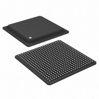
IC,DSP,32-BIT,BGA,484PIN,PLASTIC
Manufacturer
Analog Devices Inc
Series
TigerSHARC®r
Type
Fixed/Floating Pointr
Datasheet
1.ADSP-TS101SAB1-000.pdf
(48 pages)
Specifications of ADSP-TS101SAB2-000
Rohs Status
RoHS non-compliant
Interface
Host Interface, Link Port, Multi-Processor
Clock Rate
250MHz
Non-volatile Memory
External
On-chip Ram
768kB
Voltage - I/o
3.30V
Voltage - Core
1.20V
Operating Temperature
-40°C ~ 85°C
Mounting Type
Surface Mount
Package / Case
484-BGA
Package
484BGA
Numeric And Arithmetic Format
Fixed-Point|Floating-Point
Maximum Speed
250 MHz
Ram Size
768 KB
Device Million Instructions Per Second
250 MIPS
Lead Free Status / RoHS Status
Other names
ADSP-TS101SAB2000
Available stocks
Company
Part Number
Manufacturer
Quantity
Price
Company:

Part Number:
ADSP-TS101SAB2-000
Manufacturer:
MINI
Quantity:
1 400
Company:
Part Number:
ADSP-TS101SAB2-000
Manufacturer:
Analog Devices Inc
Quantity:
10 000


The IALUs have hardware support for circular buffers, bit
reverse, and zero-overhead looping. Circular buffers facilitate
efficient programming of delay lines and other data structures
required in digital signal processing, and they are commonly
used in digital filters and Fourier transforms. Each IALU pro-
vides registers for four circular buffers, so applications can set
up a total of eight circular buffers. The IALUs handle address
pointer wraparound automatically, reducing overhead, increas-
ing performance, and simplifying implementation. Circular
buffers can start and end at any memory location.
Because the IALU’s computational pipeline is one cycle deep, in
most cases, integer results are available in the next cycle. Hard-
ware (register dependency check) causes a stall if a result is
unavailable in a given cycle.
PROGRAM SEQUENCER
The ADSP-TS101S processor’s program sequencer supports:
Interrupt Controller
The DSP supports nested and non-nested interrupts. Each
interrupt type has a register in the interrupt vector table. Also,
each has a bit in both the interrupt latch register and the inter-
rupt mask register. All interrupts are fixed as either level
sensitive or edge sensitive, except the IRQ3–0 hardware inter-
rupts, which are programmable.
The DSP distinguishes between hardware interrupts and soft-
ware exceptions, handling them differently. When a software
exception occurs, the DSP aborts all other instructions in the
instruction pipe. When a hardware interrupt occurs, the DSP
continues to execute instructions already in the instruction pipe.
• A fully interruptible programming model with flexible pro-
• An eight-cycle instruction pipeline—three-cycle fetch pipe
• The supply of instruction fetch memory addresses; the
• The management of program structures and determination
• Branch prediction and a 128-entry branch target buffer
• Compact code without the requirement to align code in
gramming in assembly and C/C++ languages; handles
hardware interrupts with high throughput and no aborted
instruction cycles.
and five-cycle execution pipe—with computation results
available two cycles after operands are available.
sequencer’s instruction alignment buffer (IAB) caches up
to five fetched instruction lines waiting to execute; the pro-
gram sequencer extracts an instruction line from the IAB
and distributes it to the appropriate core component for
execution.
of program flow according to JUMP, CALL, RTI, RTS
instructions, loop structures, conditions, interrupts, and
software exceptions.
(BTB) to reduce branch delays for efficient execution of
conditional and unconditional branch instructions and
zero-overhead looping; correctly predicted branches that
are taken occur with zero-to-two overhead cycles, over-
coming the three-to-six stage branch penalty.
memory; the IAB handles alignment.
Rev. C | Page 5 of 48 | May 2009
Flexible Instruction Set
The 128-bit instruction line, which can contain up to four 32-bit
instructions, accommodates a variety of parallel operations for
concise programming. For example, one instruction line can
direct the DSP to conditionally execute a multiply, an add, and a
subtract in both computation blocks while it also branches to
another location in the program. Some key features of the
instruction set include:
ON-CHIP SRAM MEMORY
The ADSP-TS101S has 6M bits of on-chip SRAM memory,
divided into three blocks of 2M bits (64K words 32 bits). Each
block—M0, M1, and M2—can store program, data, or both, so
applications can configure memory to suit specific needs. Plac-
ing program instructions and data in different memory blocks,
however, enables the DSP to access data while performing an
instruction fetch.
The DSP’s internal and external memory
into a unified memory map, which defines the location
(address) of all elements in the system. The memory map is
divided into four memory areas—host space, external memory,
multiprocessor space, and internal memory—and each memory
space, except host memory, is subdivided into smaller memory
spaces.
Each internal memory block connects to one of the 128-bit-
wide internal buses—block M0 to bus MD0, block M1 to bus
MD1, and block M2 to bus MD2—enabling the DSP to perform
three memory transfers in the same cycle. The DSP’s internal
bus architecture provides a total memory bandwidth of
14.4G bytes per second, enabling the core and I/O to access
eight 32-bit data words (256 bits) and four 32-bit instructions
each cycle. The DSP’s flexible memory structure enables:
• Enhanced instructions for communications infrastructure
• Algebraic assembly language syntax
• Direct support for all DSP, imaging, and video arithmetic
• Branch prediction encoded in instruction, enables zero-
• Parallelism encoded in instruction line
• Conditional execution optional for all instructions
• User-defined, programmable partitioning between pro-
• DSP core and I/O access of different memory blocks in the
• DSP core access of all three memory blocks in parallel—
• Programmable partitioning of program and data memory
• Program access of all memory as 32-, 64-, or 128-bit
• Complete context switch in less than 20 cycles (66 ns)
to govern trellis decoding (for example, Viterbi and turbo
decoders) and despreading via complex correlations
types, eliminating hardware modes
overhead loops
gram and data memory
same cycle
one instruction and two data accesses
words—16-bit words with the DAB
(Figure
ADSP-TS101S
3) is organized
Related parts for ADSP-TS101SAB2-000
Image
Part Number
Description
Manufacturer
Datasheet
Request
R

Part Number:
Description:
±1.7g Dual-Axis IMEMS Accelerometer Evaluation Board
Manufacturer:
Analog Devices Inc
Datasheet:

Part Number:
Description:
Inertial Sensor Evaluation System
Manufacturer:
Analog Devices Inc
Datasheet:
Part Number:
Description:
Manufacturer:
Analog Devices Inc
Datasheet:
Part Number:
Description:
Manufacturer:
Analog Devices Inc
Datasheet:
Part Number:
Description:
Manufacturer:
Analog Devices Inc
Datasheet:
Part Number:
Description:
Manufacturer:
Analog Devices Inc
Datasheet:
Part Number:
Description:
Manufacturer:
Analog Devices Inc
Datasheet:
Part Number:
Description:
Manufacturer:
Analog Devices Inc
Datasheet:
Part Number:
Description:
Manufacturer:
Analog Devices Inc
Datasheet:
Part Number:
Description:
Manufacturer:
Analog Devices Inc
Datasheet:
Part Number:
Description:
Manufacturer:
Analog Devices Inc
Datasheet:
Part Number:
Description:
Manufacturer:
Analog Devices Inc
Datasheet:
Part Number:
Description:
Manufacturer:
Analog Devices Inc
Datasheet: