ADSP-TS101SAB2-000 Analog Devices Inc, ADSP-TS101SAB2-000 Datasheet - Page 19
ADSP-TS101SAB2-000
Manufacturer Part Number
ADSP-TS101SAB2-000
Description
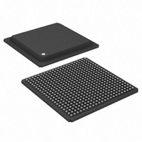
IC,DSP,32-BIT,BGA,484PIN,PLASTIC
Manufacturer
Analog Devices Inc
Series
TigerSHARC®r
Type
Fixed/Floating Pointr
Datasheet
1.ADSP-TS101SAB1-000.pdf
(48 pages)
Specifications of ADSP-TS101SAB2-000
Rohs Status
RoHS non-compliant
Interface
Host Interface, Link Port, Multi-Processor
Clock Rate
250MHz
Non-volatile Memory
External
On-chip Ram
768kB
Voltage - I/o
3.30V
Voltage - Core
1.20V
Operating Temperature
-40°C ~ 85°C
Mounting Type
Surface Mount
Package / Case
484-BGA
Package
484BGA
Numeric And Arithmetic Format
Fixed-Point|Floating-Point
Maximum Speed
250 MHz
Ram Size
768 KB
Device Million Instructions Per Second
250 MIPS
Lead Free Status / RoHS Status
Other names
ADSP-TS101SAB2000
Available stocks
Company
Part Number
Manufacturer
Quantity
Price
Company:

Part Number:
ADSP-TS101SAB2-000
Manufacturer:
MINI
Quantity:
1 400
Company:
Part Number:
ADSP-TS101SAB2-000
Manufacturer:
Analog Devices Inc
Quantity:
10 000


Table 15. Pin Definitions—Power, Ground, and Reference
STRAP PIN FUNCTION DESCRIPTIONS
Some pins have alternate functions at reset. Strap options set
DSP operating modes. During reset, the DSP samples the strap
option pins. Strap pins have an approximately 100 k pull-
down for the default value. If a strap pin is not connected to an
external pull-up or logic load, the DSP samples the default value
during reset. If strap pins are connected to logic inputs, a stron-
ger external pull-down may be required to ensure default value
Table 16. Pin Definitions—I/O Strap Pins
Signal
V
V
V
V
V
V
NC
Type column symbols: A = asynchronous; G = ground; I = input; O = output; o/d = open drain output; P = power supply;
pd = internal pull-down approximately 100 k
Term (for termination) column symbols: epd = external pull-down approximately 10 k
to V
Signal
EBOOT
IRQEN
TM1
TM2
DD
DD_A
DD_IO
REF
SS
SS_A
DD-IO
, nc = not connected; au = always used.
Type
P
P
P
I
G
G
On Pin …
BMS
BM
L2DIR
TMR0E
Term
au
au
au
au
au
au
Description
V
V
V
Reference voltage defines the trip point for all input buffers, except RESET, IRQ3–0, DMAR3–0,
ID2–0, CONTROLIMP2–0, TCK, TDI, TMS, and TRST. The value is 1.5 V ± 100 mV (which is the TTL
trip point). V
voltage divider should have an HF decoupling capacitor (1 nF HF SMD) connected to V
the decoupling capacitor between V
more information, see Filtering Reference Voltage and Clocks on Page 10.
Ground pins.
Ground pins for analog circuits.
No connect. Do not connect these pins to anything (not to any supply, signal, or each other),
because they are reserved and must be left unconnected.
DD
DD
DD
; pu = internal pull-up approximately 100 k
Description
EPROM boot.
Interrupt Enable.
Test Mode 1.
Test Mode 2.
pins for internal logic.
pins for analog circuits. Pay critical attention to bypassing this supply.
pins for I/O buffers.
0 = boot from EPROM immediately after reset (default)
1 = idle after reset and wait for an external device to boot DSP through the
0 = disable and set IRQ3–0 interrupts to level sensitive after reset (default)
1 = enable and set IRQ3–0 interrupts to edge sensitive immediately after reset
0 = required setting during reset.
1 = reserved.
0 = required setting during reset.
1 = reserved.
Rev. C | Page 19 of 48 | May 2009
external port or a link port
REF
can be connected to a power supply or set by a voltage divider circuit. The
depending on leakage and/or low level input current of the logic
load. To set a mode other than the default mode, connect the
strap pin to a sufficiently stronger external pull-up. In a multi-
processor system, up to eight DSPs may be connected on the
cluster bus, resulting in parallel combination of strap pin pull-
down resistors.
strap pins.
REF
input and V
to V
Table 16
; T = three-state
SS
; epu = external pull-up approximately 10 k
SS
, as close to the DSP’s pins as possible.
lists and describes each of the DSP’s
ADSP-TS101S
SS
. Tie
For
Related parts for ADSP-TS101SAB2-000
Image
Part Number
Description
Manufacturer
Datasheet
Request
R

Part Number:
Description:
±1.7g Dual-Axis IMEMS Accelerometer Evaluation Board
Manufacturer:
Analog Devices Inc
Datasheet:

Part Number:
Description:
Inertial Sensor Evaluation System
Manufacturer:
Analog Devices Inc
Datasheet:
Part Number:
Description:
Manufacturer:
Analog Devices Inc
Datasheet:
Part Number:
Description:
Manufacturer:
Analog Devices Inc
Datasheet:
Part Number:
Description:
Manufacturer:
Analog Devices Inc
Datasheet:
Part Number:
Description:
Manufacturer:
Analog Devices Inc
Datasheet:
Part Number:
Description:
Manufacturer:
Analog Devices Inc
Datasheet:
Part Number:
Description:
Manufacturer:
Analog Devices Inc
Datasheet:
Part Number:
Description:
Manufacturer:
Analog Devices Inc
Datasheet:
Part Number:
Description:
Manufacturer:
Analog Devices Inc
Datasheet:
Part Number:
Description:
Manufacturer:
Analog Devices Inc
Datasheet:
Part Number:
Description:
Manufacturer:
Analog Devices Inc
Datasheet:
Part Number:
Description:
Manufacturer:
Analog Devices Inc
Datasheet: