ADSP-TS101SAB2-000 Analog Devices Inc, ADSP-TS101SAB2-000 Datasheet - Page 21
ADSP-TS101SAB2-000
Manufacturer Part Number
ADSP-TS101SAB2-000
Description
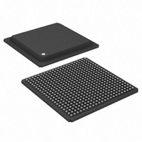
IC,DSP,32-BIT,BGA,484PIN,PLASTIC
Manufacturer
Analog Devices Inc
Series
TigerSHARC®r
Type
Fixed/Floating Pointr
Datasheet
1.ADSP-TS101SAB1-000.pdf
(48 pages)
Specifications of ADSP-TS101SAB2-000
Rohs Status
RoHS non-compliant
Interface
Host Interface, Link Port, Multi-Processor
Clock Rate
250MHz
Non-volatile Memory
External
On-chip Ram
768kB
Voltage - I/o
3.30V
Voltage - Core
1.20V
Operating Temperature
-40°C ~ 85°C
Mounting Type
Surface Mount
Package / Case
484-BGA
Package
484BGA
Numeric And Arithmetic Format
Fixed-Point|Floating-Point
Maximum Speed
250 MHz
Ram Size
768 KB
Device Million Instructions Per Second
250 MIPS
Lead Free Status / RoHS Status
Other names
ADSP-TS101SAB2000
Available stocks
Company
Part Number
Manufacturer
Quantity
Price
Company:

Part Number:
ADSP-TS101SAB2-000
Manufacturer:
MINI
Quantity:
1 400
Company:
Part Number:
ADSP-TS101SAB2-000
Manufacturer:
Analog Devices Inc
Quantity:
10 000


ABSOLUTE MAXIMUM RATINGS
Stresses greater than those listed in
nent damage to the device. These are stress ratings only;
functional operation of the device at these or any other condi-
tions greater than those indicated in the operational sections of
this specification is not implied. Exposure to absolute maximum
rating conditions for extended periods may affect device
reliability.
Table 17. Absolute Maximum Ratings
ESD CAUTION
PACKAGE INFORMATION
The information presented in
package branding for the ADSP-TS101S processors. For a com-
plete listing of product availability, see
Page
Parameter
Internal (Core) Supply Voltage (V
Analog (PLL) Supply Voltage (V
External (I/O) Supply Voltage (V
Input Voltage
Output Voltage Swing
Storage Temperature Range
45.
ESD (electrostatic discharge) sensitive device.
Charged devices and circuit boards can discharge
without detection. Although this product features
patented or proprietary protection circuitry, damage
may occur on devices subjected to high energy ESD.
Therefore, proper ESD precautions should be taken to
avoid performance degradation or loss of functionality.
Figure 7. Typical Package Brand
yyww country_of_origin
a
LLLLLLLLL-L 2.0
ADSP-TS101S
T
tppZ-ccc
Figure 7
DD_A
DDEXT
DDINT
)
Table 19
)
)
provide details about the
Ordering Guide on
vvvvv
Rating
–0.3 V to +1.40 V
–0.3 V to +1.40 V
–0.3 V to +4.6 V
–0.5 V to V
–0.5 V to V
–65C to +150C
may cause perma-
Rev. C | Page 21 of 48 | May 2009
DD
DD
_IO
_IO
+ 0.5 V
+ 0.5 V
Table 18. Package Brand Information
TIMING SPECIFICATIONS
With the exception of link port, IRQ3–0, DMAR3–0, TMR0E,
FLAG3–0 (input), and TRST pins, all ac timing for the ADSP-
TS101S is relative to a reference clock edge. Because input
setup/hold, output valid/hold, and output enable/disable times
are relative to a clock edge, the timing data for the ADSP-
TS101S has few calculated (formula-based) values. For informa-
tion on ac timing, see
link port transfer timing, see
Token Switch Timing on Page
General AC Timing
Timing is measured on signals when they cross the 1.5 V level as
described in
are measured between the point that the first signal reaches
1.5 V and the point that the second signal reaches 1.5 V.
The ac asynchronous timing data for the IRQ3–0, DMAR3–0,
TMR0E, FLAG3–0 (input), and TRST pins appears in
The general ac timing data appears in
Table
fied in
strength 4. Output valid and hold are based on standard capaci-
tive loads: 30 pF on all pins. The delay and hold specifications
given should be derated by a drive strength related factor for
loads other than the nominal value of 30 pF.
In order to calculate the output valid and hold times for differ-
ent load conditions and/or output drive strengths, refer to
Figure 32 on Page 34
Fall Time vs. Load Capacitance) and
put Valid vs. Load Capacitance and Drive Strength).
Brand Key
t
pp
Z
ccc
LLLLLLLLL-L
R.R
yyww
vvvvvv
30. All ac specifications are measured with the load speci-
Figure
Figure 8. Equivalent Device Loading for AC Measurements
(Includes All Fixtures)
Figure 16 on Page
8, and with the output drive strength set to
OUTPUT
PIN
TO
through
General AC
Field Description
Temperature Range
Package Type
Lead Free Option (optional)
See Ordering Guide
Silicon Lot Number
Silicon Revision
Date Code
Assembly Lot Code
Link Ports Data Transfer and
30pF
Figure 39 on Page 36
29.
28. All delays (in nanoseconds)
Timing. For information on
50
Figure 40 on Page 36
Table
ADSP-TS101S
1.5V
21,
Table
(Rise and
29, and
Table
(Out-
21.
Related parts for ADSP-TS101SAB2-000
Image
Part Number
Description
Manufacturer
Datasheet
Request
R

Part Number:
Description:
±1.7g Dual-Axis IMEMS Accelerometer Evaluation Board
Manufacturer:
Analog Devices Inc
Datasheet:

Part Number:
Description:
Inertial Sensor Evaluation System
Manufacturer:
Analog Devices Inc
Datasheet:
Part Number:
Description:
Manufacturer:
Analog Devices Inc
Datasheet:
Part Number:
Description:
Manufacturer:
Analog Devices Inc
Datasheet:
Part Number:
Description:
Manufacturer:
Analog Devices Inc
Datasheet:
Part Number:
Description:
Manufacturer:
Analog Devices Inc
Datasheet:
Part Number:
Description:
Manufacturer:
Analog Devices Inc
Datasheet:
Part Number:
Description:
Manufacturer:
Analog Devices Inc
Datasheet:
Part Number:
Description:
Manufacturer:
Analog Devices Inc
Datasheet:
Part Number:
Description:
Manufacturer:
Analog Devices Inc
Datasheet:
Part Number:
Description:
Manufacturer:
Analog Devices Inc
Datasheet:
Part Number:
Description:
Manufacturer:
Analog Devices Inc
Datasheet:
Part Number:
Description:
Manufacturer:
Analog Devices Inc
Datasheet: