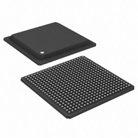
ADSP-TS101SAB2-000 Analog Devices Inc, ADSP-TS101SAB2-000 Datasheet - Page 7

ADSP-TS101SAB2-000
Manufacturer Part Number
ADSP-TS101SAB2-000
Description
IC,DSP,32-BIT,BGA,484PIN,PLASTIC
Manufacturer
Analog Devices Inc
Series
TigerSHARC®r
Type
Fixed/Floating Pointr
Datasheet
1.ADSP-TS101SAB1-000.pdf
(48 pages)
Specifications of ADSP-TS101SAB2-000
Rohs Status
RoHS non-compliant
Interface
Host Interface, Link Port, Multi-Processor
Clock Rate
250MHz
Non-volatile Memory
External
On-chip Ram
768kB
Voltage - I/o
3.30V
Voltage - Core
1.20V
Operating Temperature
-40°C ~ 85°C
Mounting Type
Surface Mount
Package / Case
484-BGA
Package
484BGA
Numeric And Arithmetic Format
Fixed-Point|Floating-Point
Maximum Speed
250 MHz
Ram Size
768 KB
Device Million Instructions Per Second
250 MIPS
Lead Free Status / RoHS Status
Other names
ADSP-TS101SAB2000
Available stocks
Company
Part Number
Manufacturer
Quantity
Price
Company:
Part Number:
ADSP-TS101SAB2-000
Manufacturer:
MINI
Quantity:
1 400
Company:
Part Number:
ADSP-TS101SAB2-000
Manufacturer:
Analog Devices Inc
Quantity:
10 000
Host Interface
The ADSP-TS101S provides an easy and configurable interface
between its external bus and host processors through the exter-
nal port. To accommodate a variety of host processors, the host
interface supports pipelined or slow protocols for accesses of the
host as slave. Each protocol has programmable transmission
parameters, such as idle cycles, pipe depth, and internal
wait cycles.
The host interface supports burst transactions initiated by a host
processor. After the host issues the starting address of the burst
and asserts the BRST signal, the DSP increments the address
internally while the host continues to assert BRST.
The host interface provides a deadlock recovery mechanism that
enables a host to recover from deadlock situations involving the
DSP. The BOFF signal provides the deadlock recovery mecha-
nism. When the host asserts BOFF, the DSP backs off the
current transaction and asserts HBG and relinquishes the exter-
nal bus.
The host can directly read or write the internal memory of the
ADSP-TS101S, and it can access most of the DSP registers,
including DMA control (TCB) registers. Vector interrupts sup-
port efficient execution of host commands.
Multiprocessor Interface
The ADSP-TS101S offers powerful features tailored to multi-
processing DSP systems through the external port and link
ports. This multiprocessing capability provides highest band-
width for interprocessor communication, including:
The external port and link ports provide integrated, glueless
multiprocessing support.
The external port supports a unified address space (see
that enables direct interprocessor accesses of each
ADSP-TS101S processor’s internal memory and registers. The
DSP’s on-chip distributed bus arbitration logic provides simple,
glueless connection for systems containing up to eight ADSP-
TS101S processors and a host processor. Bus arbitration has a
rotating priority. Bus lock supports indivisible read-modify-
write sequences for semaphores. A bus fairness feature prevents
one DSP from holding the external bus too long.
The DSP’s four link ports provide a second path for interproces-
sor communications with throughput of 1G bytes per second.
The cluster bus provides 800M bytes per second throughput—
with a total of 1.8G bytes per second interprocessor bandwidth.
SDRAM Controller
The SDRAM controller controls the ADSP-TS101S processor’s
transfers of data to and from synchronous DRAM (SDRAM).
The throughput is 32 or 64 bits per SCLK cycle using the exter-
nal port and SDRAM control pins.
• Up to eight DSPs on a common bus
• On-chip arbitration for glueless multiprocessing
• Link ports for point-to-point communication
Rev. C | Page 7 of 48 | May 2009
Figure
3)
The SDRAM interface provides a glueless interface with stan-
dard SDRAMs—16M bit, 64M bit, 128M bit, and 256M bit. The
DSP directly supports a maximum of 64M words 32 bits of
SDRAM. The SDRAM interface is mapped in external memory
in the DSP’s unified memory map.
EPROM Interface
The ADSP-TS101S can be configured to boot from external
8-bit EPROM at reset through the external port. An automatic
process (which follows reset) loads a program from the EPROM
into internal memory. This process uses 16 wait cycles for each
read access. During booting, the BMS pin functions as the
EPROM chip select signal. The EPROM boot procedure uses
DMA Channel 0, which packs the bytes into 32-bit instructions.
Applications can also access the EPROM (write flash memories)
during normal operation through DMA.
The EPROM or flash memory interface is not mapped in the
DSP’s unified memory map. It is a byte address space limited to
a maximum of 16M bytes (24 address bits). The EPROM or
flash memory interface can be used after boot via a DMA.
DMA CONTROLLER
The ADSP-TS101S processor’s on-chip DMA controller, with
14 DMA channels, provides zero-overhead data transfers with-
out processor intervention. The DMA controller operates
independently and invisibly to the DSP’s core, enabling DMA
operations to occur while the DSP’s core continues to execute
program instructions. The DMA controller performs DMA
transfers between:
The DMA controller provides a number of additional features.
The DMA controller supports flyby transfers. Flyby operations
only occur through the external port (DMA Channel 0) and do
not involve the DSP’s core. The DMA controller acts as a con-
duit to transfer data from one external device to another
through external memory. During a transaction, the DSP:
DMA chaining is also supported by the DMA controller. DMA
chaining operations enable applications to automatically link
one DMA transfer sequence to another for continuous trans-
mission. The sequences can occur over different DMA channels
and have different transmission attributes.
• Internal memory and external memory and memory-
• Internal memory of other DSPs on a common bus, a host
• External memory and external peripherals or link port I/O
• External bus master and internal memory or link port I/O
• Relinquishes the external data bus
• Outputs addresses, memory selects (MS1–0, MSSD, RAS,
• Responds to ACK
mapped peripherals
processor, or link port I/O
CAS, and SDWE) and the FLYBY, IOEN, and RD/WR
strobes
ADSP-TS101S


