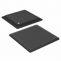
ADSP-TS101SAB2-000 Analog Devices Inc, ADSP-TS101SAB2-000 Datasheet - Page 34

ADSP-TS101SAB2-000
Manufacturer Part Number
ADSP-TS101SAB2-000
Description
IC,DSP,32-BIT,BGA,484PIN,PLASTIC
Manufacturer
Analog Devices Inc
Series
TigerSHARC®r
Type
Fixed/Floating Pointr
Datasheet
1.ADSP-TS101SAB1-000.pdf
(48 pages)
Specifications of ADSP-TS101SAB2-000
Rohs Status
RoHS non-compliant
Interface
Host Interface, Link Port, Multi-Processor
Clock Rate
250MHz
Non-volatile Memory
External
On-chip Ram
768kB
Voltage - I/o
3.30V
Voltage - Core
1.20V
Operating Temperature
-40°C ~ 85°C
Mounting Type
Surface Mount
Package / Case
484-BGA
Package
484BGA
Numeric And Arithmetic Format
Fixed-Point|Floating-Point
Maximum Speed
250 MHz
Ram Size
768 KB
Device Million Instructions Per Second
250 MIPS
Lead Free Status / RoHS Status
Other names
ADSP-TS101SAB2000
Available stocks
Company
Part Number
Manufacturer
Quantity
Price
Company:
Part Number:
ADSP-TS101SAB2-000
Manufacturer:
MINI
Quantity:
1 400
Company:
Part Number:
ADSP-TS101SAB2-000
Manufacturer:
Analog Devices Inc
Quantity:
10 000
ADSP-TS101S
TEST CONDITIONS
The test conditions for timing parameters appearing in
on Page 29
output enable time, and capacitive loading. The timing specifi-
cations for the DSP apply for the voltage reference levels in
Figure
Output Disable Time
Output pins are considered to be disabled when they stop driv-
ing, go into a high impedance state, and start to decay from their
output high or low voltage. The time for the voltage on the bus
to decay by V is dependent on the capacitive load, C
load current, I
lowing equation:
The output disable time t
t
t
switches to when the output voltage decays V from the mea-
sured output high or output low voltage. The t
calculated with test loads C
Output Enable Time
Output pins are considered to be enabled when they have made
a transition from a high impedance state to when they start driv-
ing. The time for the voltage on the bus to ramp by
dependent on the capacitive load, C
This ramp time can be approximated by the following equation:
MEASURED_DIS
MEASURED_DIS
REFERENCE
OUTPUT
V
V
29.
OL (MEASURED)
OH (MEASURED)
INPUT
SIGNAL
OR
and
Figure 29. Voltage Reference Levels for AC Measurements
and t
is the interval from when the reference signal
L
1.5V
. This decay time can be approximated by the fol-
Table 30 on Page 30
t
DIS
Figure 30. Output Enable/Disable
DECAY
OUTPUT STOPS
t
MEASURED_DIS
DRIVING
t
(Except Output Enable/Disable)
DECAY
as shown in
VOLTAGE TO BE APPROXIMATELY 1.5V.
DIS
L
V
V
TEST CONDITIONS CAUSE THIS
is the difference between
and I
OH (MEASURED)
OL (MEASURED)
t
DECAY
HIGH IMPEDANCE STATE.
=
L
, and with V equal to 0.5 V.
C L V
-------------- -
L
include output disable time,
Figure
, and the drive current, I
I L
+ V
– V
t
ENA
30. The time
t
t
OUTPUT STARTS
RAMP
MEASURED_ENA
DECAY
2.0V
1.0V
DRIVING
value is
1.5V
Rev. C | Page 34 of 48 | May 2009
V is
L
Table 29
and the
D
.
The output enable time t
t
t
switches to when the output voltage ramps V from the mea-
sured three-stated output level. The t
with test load C
Capacitive Loading
Figure 31
used for measuring typical output rise and fall times.
through
itance.
load capacitance. (Note that this graph or derating does not
apply to output disable delays; see
Page
linear outside the ranges shown.
MEASURED_ENA
MEASURED_ENA
Figure 32. Typical Output Rise and Fall Time (10%–90%, V
34.) The graphs of
25
20
15
10
Figure 40
5
0
Figure 39
0
shows the circuit with variable capacitance that is
Figure 31. Equivalent Device Loading for AC Measurements
y = 0.2015x + 3.8869
10
and t
is the interval from when the reference signal
OUTPUT
L
PIN
, drive current I
TO
RISE TIME
graphically shows how output valid varies with
20
RAMP
show how output rise time varies with capac-
vs. Load Capacitance at Strength 0
30
t
LOAD CAPACITANCE (pF)
as shown in
RAMP
Figure 32
ENA
(V
40
(Includes All Fixtures)
STRENGTH 0
DD_IO
is the difference between
(10pF to 100pF)
VARIABLE
50
=
D
= 3.3V)
, and with V equal to 0.5 V.
through
Output Disable Time on
C
-------------- -
60
Figure
L
I D
RAMP
V
70
y = 0.174x + 2.6931
value is calculated
Figure 40
30. The time
1.5V
FALL TIME
80
90
100
DD_IO
may not be
Figure 32
= 3.3 V)


