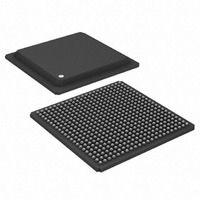
ADSP-TS101SAB2-000 Analog Devices Inc, ADSP-TS101SAB2-000 Datasheet - Page 22

ADSP-TS101SAB2-000
Manufacturer Part Number
ADSP-TS101SAB2-000
Description
IC,DSP,32-BIT,BGA,484PIN,PLASTIC
Manufacturer
Analog Devices Inc
Series
TigerSHARC®r
Type
Fixed/Floating Pointr
Datasheet
1.ADSP-TS101SAB1-000.pdf
(48 pages)
Specifications of ADSP-TS101SAB2-000
Rohs Status
RoHS non-compliant
Interface
Host Interface, Link Port, Multi-Processor
Clock Rate
250MHz
Non-volatile Memory
External
On-chip Ram
768kB
Voltage - I/o
3.30V
Voltage - Core
1.20V
Operating Temperature
-40°C ~ 85°C
Mounting Type
Surface Mount
Package / Case
484-BGA
Package
484BGA
Numeric And Arithmetic Format
Fixed-Point|Floating-Point
Maximum Speed
250 MHz
Ram Size
768 KB
Device Million Instructions Per Second
250 MIPS
Lead Free Status / RoHS Status
Other names
ADSP-TS101SAB2000
Available stocks
Company
Part Number
Manufacturer
Quantity
Price
Company:
Part Number:
ADSP-TS101SAB2-000
Manufacturer:
MINI
Quantity:
1 400
Company:
Part Number:
ADSP-TS101SAB2-000
Manufacturer:
Analog Devices Inc
Quantity:
10 000
ADSP-TS101S
For power-up sequencing, power-up reset, and normal reset
(hot reset) timing requirements, refer to
Table 27
respectively.
Table 19. AC Asynchronous Signal Specifications (All values in this table are in nanoseconds)
1
2
3
Table 20. Reference Clocks—Core Clock (CCLK) Cycle Time
1
Table 21. Reference Clocks—Local Clock (LCLK) Cycle Time
1
2
3
4
5
6
Name
IRQ3–0
DMAR3–0
TMR0E
FLAG3–0
TRST
Parameter
t
Parameter
t
t
t
t
These input pins do not need to be synchronized to a clock reference.
This pin is a strap option. During reset, an internal resistor pulls the pin low.
For output specifications, see
CCLK is the internal processor clock or instruction cycle time. The period of this clock is equal to the system clock period (t
For more information, see
For more information, see Clock Domains on Page 9.
LCLK_P and SCLK_P must be connected to the same source.
The value of (t
Actual input jitter should be combined with ac specifications for accurate timing analysis.
Jitter specification is maximum peak-to-peak time interval error (TIE) jitter.
CCLK
LCLK
LCLKH
LCLKL
LCLKJ
(SCLKRAT2–0). For information on available part numbers for different internal processor clock rates, see the
1, 2, 3, 4
1
5, 6
2
1
and
1, 3
1
LCLK
LCLK_P
CCLK
Figure
LCLK_P
/ LCLKRAT2-0) must not violate the specification for t
Description
Core Clock Cycle Time
Description
Local Clock Cycle Time
Local Clock Cycle High Time
Local Clock Cycle Low Time
Local Clock Jitter Tolerance
14, and
Table 3 on Page
Table 29
Table
and
28, and
Interrupt request input
DMA request input
Timer 0 expired output
Flag pins input
JTAG test reset input
Description
Table
12.
Table 26
30.
Figure 15
Figure 10. Reference Clocks—Local Clock (LCLK) Cycle Time
Figure 9. Reference Clocks—Core Clock (CCLK) Cycle Time
t
t
LCLKH
LCLKH
and
t
CCLK
t
t
Rev. C | Page 22 of 48 | May 2009
LCLK
LCLK
Figure
t
t
LCLKL
LCLKL
CCLK
13,
.
Pulse Width Low (min)
t
t
3 t
1 ns
Min
3.3
CCLK
CCLK
Grade = 100 (300 MHz)
CCLK
+ 3 ns
+ 4 ns
ns
Max
12.5
t
t
LCLKJ
LCLKJ
Ordering Guide on Page
Min
4.0
Min
0.4 × t
10
0.4 × t
SCLK
Grade = 000 (250 MHz)
) divided by the system clock ratio
Pulse Width High (min)
t
4 t
3 t
CCLK
LCLK
LCLK
SCLK
CCLK
+ 4 ns
45.
ns
ns
Max
12.5
Max
25
0.6 × t
0.6 × t
500
LCLK
LCLK
Unit
ns
Unit
ns
ns
ns
ps


