ADSP-TS101SAB2-000 Analog Devices Inc, ADSP-TS101SAB2-000 Datasheet - Page 3
ADSP-TS101SAB2-000
Manufacturer Part Number
ADSP-TS101SAB2-000
Description
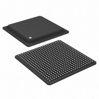
IC,DSP,32-BIT,BGA,484PIN,PLASTIC
Manufacturer
Analog Devices Inc
Series
TigerSHARC®r
Type
Fixed/Floating Pointr
Datasheet
1.ADSP-TS101SAB1-000.pdf
(48 pages)
Specifications of ADSP-TS101SAB2-000
Rohs Status
RoHS non-compliant
Interface
Host Interface, Link Port, Multi-Processor
Clock Rate
250MHz
Non-volatile Memory
External
On-chip Ram
768kB
Voltage - I/o
3.30V
Voltage - Core
1.20V
Operating Temperature
-40°C ~ 85°C
Mounting Type
Surface Mount
Package / Case
484-BGA
Package
484BGA
Numeric And Arithmetic Format
Fixed-Point|Floating-Point
Maximum Speed
250 MHz
Ram Size
768 KB
Device Million Instructions Per Second
250 MIPS
Lead Free Status / RoHS Status
Other names
ADSP-TS101SAB2000
Available stocks
Company
Part Number
Manufacturer
Quantity
Price
Company:

Part Number:
ADSP-TS101SAB2-000
Manufacturer:
MINI
Quantity:
1 400
Company:
Part Number:
ADSP-TS101SAB2-000
Manufacturer:
Analog Devices Inc
Quantity:
10 000


GENERAL DESCRIPTION
The ADSP-TS101S TigerSHARC
formance, Static Superscalar
signal processing tasks and communications infrastructure. The
DSP combines very wide memory widths with dual computa-
tion blocks—supporting 32- and 40-bit floating-point and 8-,
16-, 32-, and 64-bit fixed-point processing—to set a new stan-
dard of performance for digital signal processors. The
TigerSHARC processor’s Static Superscalar architecture lets the
processor execute up to four instructions each cycle, performing
24 fixed-point (16-bit) operations or six floating-point
operations.
Three independent 128-bit-wide internal data buses, each
connecting to one of the three 2M bit memory banks, enable
quad word data, instruction, and I/O accesses and provide
14.4G bytes per second of internal memory bandwidth. Operat-
ing at 300 MHz, the ADSP-TS101S processor’s core has a 3.3 ns
instruction cycle time. Using its single-instruction, multiple-
data (SIMD) features, the ADSP-TS101S can perform 2.4 billion
40-bit MACs or 600 million 80-bit MACs per second.
and
Table 1. General-Purpose Algorithm Benchmarks
at 300 MHz
Table 2. 3G Wireless Algorithm Benchmarks
1
†
Benchmark
32-bit algorithm, 600 million MACs/s peak performance
1024 point complex FFT (Radix 2)
50-tap FIR on 1024 input
Single FIR MAC
16-bit algorithm, 2.4 billion MACs/s peak performance
256 point complex FFT (Radix 2)
50-tap FIR on 1024 input
Single FIR MAC
Single complex FIR MAC
I/O DMA transfer rate
External port
Link ports (each)
Benchmark
Turbo decode
Viterbi decode
Complex correlation
The execution speed is in instruction cycles per second.
Static Superscalar is a trademark of Analog Devices, Inc.
3.84 Mcps
384 kbps data channel
12.2 kbps AMR
Table 2
show the DSP’s performance benchmarks.
4
with a spreading factor of 256
3
voice channel
TM
†
processor optimized for large
®
processor is an ultrahigh per-
Speed
32.78 μs
91.67 μs
1.83 ns
3.67 μs
24.0 μs
0.47 ns
1.9 ns
800M bytes/s
250M bytes/s
Execution
(MIPS)
51 MIPS
0.86 MIPS
0.27 MIPS
Rev. C | Page 3 of 48 | May 2009
Table 1
Clock
Cycles
9,835
27,500
0.55
1,100
7,200
0.14
0.57
n/a
n/a
1
2
2
3
4
The ADSP-TS101S is code compatible with the other
TigerSHARC processors.
The Functional Block Diagram on
architectural blocks. These blocks include:
Figure 2
SDRAM.
system.
The TigerSHARC processor uses a Static Superscalar architec-
ture. This architecture is superscalar in that the ADSP-TS101S
processor’s core can execute simultaneously from one to four
32-bit instructions encoded in a very large instruction word
(VLIW) instruction line using the DSP’s dual compute blocks.
Because the DSP does not perform instruction reordering at
runtime—the programmer selects which operations will execute
in parallel prior to runtime—the order of instructions is static.
With few exceptions, an instruction line, whether it contains
one, two, three, or four 32-bit instructions, executes with a
throughput of one cycle in an eight-deep processor pipeline.
For optimal DSP program execution, programmers must follow
the DSP’s set of instruction parallelism rules when encoding an
instruction line. In general, the selection of instructions that the
DSP can execute in parallel each cycle depends on the instruc-
tion line resources each instruction requires and on the source
and destination registers used in the instructions. The program-
mer has direct control of three core components—the IALUs,
the compute blocks, and the program sequencer.
This value is for six iterations of the algorithm. For eight iterations of the turbo
Adaptive multi rate (AMR)
Megachips per second (Mcps)
decoder, this benchmark is 67 MIPS.
• Dual compute blocks, each consisting of an ALU, multi-
• Dual integer ALUs (IALUs), each with its own 31-word
• A program sequencer with instruction alignment buffer
• Three 128-bit internal data buses, each connecting to one
• On-chip SRAM (6M bit)
• An external port that provides the interface to host proces-
• A 14-channel DMA controller
• Four link ports
• Two 64-bit interval timers and timer expired pin
• A 1149.1 IEEE compliant JTAG test access port for on-chip
plier, 64-bit shifter, and 32-word register file and associated
data alignment buffers (DABs)
register file for data addressing
(IAB), branch target buffer (BTB), and interrupt controller
of three 2M bit memory banks
sors, multiprocessing space (DSPs), off-chip memory-
mapped peripherals, and external SRAM and SDRAM
emulation
shows a typical single-processor system with external
Figure 4 on Page 8
shows a typical multiprocessor
Page 1
shows the processor’s
ADSP-TS101S
Related parts for ADSP-TS101SAB2-000
Image
Part Number
Description
Manufacturer
Datasheet
Request
R

Part Number:
Description:
±1.7g Dual-Axis IMEMS Accelerometer Evaluation Board
Manufacturer:
Analog Devices Inc
Datasheet:

Part Number:
Description:
Inertial Sensor Evaluation System
Manufacturer:
Analog Devices Inc
Datasheet:
Part Number:
Description:
Manufacturer:
Analog Devices Inc
Datasheet:
Part Number:
Description:
Manufacturer:
Analog Devices Inc
Datasheet:
Part Number:
Description:
Manufacturer:
Analog Devices Inc
Datasheet:
Part Number:
Description:
Manufacturer:
Analog Devices Inc
Datasheet:
Part Number:
Description:
Manufacturer:
Analog Devices Inc
Datasheet:
Part Number:
Description:
Manufacturer:
Analog Devices Inc
Datasheet:
Part Number:
Description:
Manufacturer:
Analog Devices Inc
Datasheet:
Part Number:
Description:
Manufacturer:
Analog Devices Inc
Datasheet:
Part Number:
Description:
Manufacturer:
Analog Devices Inc
Datasheet:
Part Number:
Description:
Manufacturer:
Analog Devices Inc
Datasheet:
Part Number:
Description:
Manufacturer:
Analog Devices Inc
Datasheet: