ADSP-TS101SAB2-000 Analog Devices Inc, ADSP-TS101SAB2-000 Datasheet - Page 8
ADSP-TS101SAB2-000
Manufacturer Part Number
ADSP-TS101SAB2-000
Description
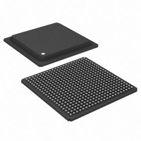
IC,DSP,32-BIT,BGA,484PIN,PLASTIC
Manufacturer
Analog Devices Inc
Series
TigerSHARC®r
Type
Fixed/Floating Pointr
Datasheet
1.ADSP-TS101SAB1-000.pdf
(48 pages)
Specifications of ADSP-TS101SAB2-000
Rohs Status
RoHS non-compliant
Interface
Host Interface, Link Port, Multi-Processor
Clock Rate
250MHz
Non-volatile Memory
External
On-chip Ram
768kB
Voltage - I/o
3.30V
Voltage - Core
1.20V
Operating Temperature
-40°C ~ 85°C
Mounting Type
Surface Mount
Package / Case
484-BGA
Package
484BGA
Numeric And Arithmetic Format
Fixed-Point|Floating-Point
Maximum Speed
250 MHz
Ram Size
768 KB
Device Million Instructions Per Second
250 MIPS
Lead Free Status / RoHS Status
Other names
ADSP-TS101SAB2000
Available stocks
Company
Part Number
Manufacturer
Quantity
Price
Company:

Part Number:
ADSP-TS101SAB2-000
Manufacturer:
MINI
Quantity:
1 400
Company:
Part Number:
ADSP-TS101SAB2-000
Manufacturer:
Analog Devices Inc
Quantity:
10 000


ADSP-TS101S
The DMA controller also supports two-dimensional transfers.
The DMA controller can access and transfer two-dimensional
memory arrays on any DMA transmit or receive channel. These
transfers are implemented with index, count, and modify regis-
ters for both the X and Y dimensions.
The DMA controller performs the following DMA operations:
• External port block transfers. Four dedicated bidirectional
• Link port transfers. Eight dedicated DMA channels (four
DMA channels transfer blocks of data between the DSP’s
internal memory and any external memory or memory-
mapped peripheral on the external bus. These transfers
support master mode and handshake mode protocols.
transmit and four receive) transfer quad word data only
between link ports and between a link port and internal or
REFERENCE
(OPTIONAL)
VOLTAGE
DEVICES
(4 MAX)
CLOCK
RESET
LINK
000
001
LXDAT7–0
LXCLKIN
LXCLKOUT
LXDIR
TMR0E
BM
CONTROLIMP2–0
DS2–0
Figure 4. Shared Memory Multiprocessing System
LINK
CLKS/REFS
ID2–0
RESET
SCLK_P
LCLK_P
S/LCLK_N
V
LCLKRAT2–0
SCLKFREQ
IRQ3–0
FLAG3–0
ID2–0
CLKS/REFS
RESET
Rev. C | Page 8 of 48 | May 2009
REF
LINK
ADSP-TS101 #1
ADSP-TS101 #0
ADSP-TS101 #7
ADSP-TS101 #6
ADSP-TS101 #5
ADSP-TS101 #4
ADSP-TS101 #3
ADSP-TS101 #2
CONTROL
ADDR31–0
CONTROL
ADDR31–0
DATA63–0
DATA63–0
BUSLOCK
DMAR3–0
BR7–2,0
FLYBY
SDCKE
WRH/L
BR7–1
MS1–0
SDWE
SDA10
MSSD
HDQM
BRST
LDQM
BOFF
IOEN
MSH
HBR
HBG
RAS
CAS
ACK
BMS
BR1
BR0
CPA
DPA
RD
• AutoDMA transfers. Two dedicated unidirectional DMA
external memory. These transfers only use handshake
mode protocol. DMA priority rotates between the four
receive channels.
channels transfer data received from an external bus master
to internal memory or to link port I/O. These transfers only
use slave mode protocol, and an external bus master must
initiate the transfer.
ADDR
DATA
CS
RAS
CAS
WE
CKE
A10
ADDR
DATA
OE
WE
ACK
CS
CS
ADDR
DATA
ADDR
DATA
DQM
PERIPHERALS
(OPTIONAL)
PROCESSOR
(OPTIONAL)
(OPTIONAL)
INTERFACE
(OPTIONAL)
MEMORY
GLOBAL
MEMORY
EPROM
SDRAM
AND
BOOT
HOST
CLOCK
CLK
Related parts for ADSP-TS101SAB2-000
Image
Part Number
Description
Manufacturer
Datasheet
Request
R

Part Number:
Description:
±1.7g Dual-Axis IMEMS Accelerometer Evaluation Board
Manufacturer:
Analog Devices Inc
Datasheet:

Part Number:
Description:
Inertial Sensor Evaluation System
Manufacturer:
Analog Devices Inc
Datasheet:
Part Number:
Description:
Manufacturer:
Analog Devices Inc
Datasheet:
Part Number:
Description:
Manufacturer:
Analog Devices Inc
Datasheet:
Part Number:
Description:
Manufacturer:
Analog Devices Inc
Datasheet:
Part Number:
Description:
Manufacturer:
Analog Devices Inc
Datasheet:
Part Number:
Description:
Manufacturer:
Analog Devices Inc
Datasheet:
Part Number:
Description:
Manufacturer:
Analog Devices Inc
Datasheet:
Part Number:
Description:
Manufacturer:
Analog Devices Inc
Datasheet:
Part Number:
Description:
Manufacturer:
Analog Devices Inc
Datasheet:
Part Number:
Description:
Manufacturer:
Analog Devices Inc
Datasheet:
Part Number:
Description:
Manufacturer:
Analog Devices Inc
Datasheet:
Part Number:
Description:
Manufacturer:
Analog Devices Inc
Datasheet: