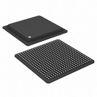
ADSP-TS101SAB2-000 Analog Devices Inc, ADSP-TS101SAB2-000 Datasheet - Page 13

ADSP-TS101SAB2-000
Manufacturer Part Number
ADSP-TS101SAB2-000
Description
IC,DSP,32-BIT,BGA,484PIN,PLASTIC
Manufacturer
Analog Devices Inc
Series
TigerSHARC®r
Type
Fixed/Floating Pointr
Datasheet
1.ADSP-TS101SAB1-000.pdf
(48 pages)
Specifications of ADSP-TS101SAB2-000
Rohs Status
RoHS non-compliant
Interface
Host Interface, Link Port, Multi-Processor
Clock Rate
250MHz
Non-volatile Memory
External
On-chip Ram
768kB
Voltage - I/o
3.30V
Voltage - Core
1.20V
Operating Temperature
-40°C ~ 85°C
Mounting Type
Surface Mount
Package / Case
484-BGA
Package
484BGA
Numeric And Arithmetic Format
Fixed-Point|Floating-Point
Maximum Speed
250 MHz
Ram Size
768 KB
Device Million Instructions Per Second
250 MIPS
Lead Free Status / RoHS Status
Other names
ADSP-TS101SAB2000
Available stocks
Company
Part Number
Manufacturer
Quantity
Price
Company:
Part Number:
ADSP-TS101SAB2-000
Manufacturer:
MINI
Quantity:
1 400
Company:
Part Number:
ADSP-TS101SAB2-000
Manufacturer:
Analog Devices Inc
Quantity:
10 000
Table 5. Pin Definitions—External Port Bus Controls
Signal
ADDR31–0
DATA63–0
RD
WRL
WRH
ACK
BMS
MS1–0
Type column symbols: A = asynchronous; G = ground; I = input; O = output; o/d = open drain output; P = power supply;
pd = internal pull-down approximately 100 k
Term (for termination) column symbols: epd = external pull-down approximately 10 k
to V
2
DD-IO
2
2, 4
2
2
, nc = not connected; au = always used.
1
1
Type
I/O/T
I/O/T
I/O/T (pu
I/O/T (pu
I/O/T (pu
I/O/T
O/T
(pu/pd
O/T (pu
3
3
)
)
3
3
3
)
)
)
Term
nc
nc
nc
nc
epu
au
nc
nc
Description
Address Bus. The DSP issues addresses for accessing memory and peripherals on these pins. In
a multiprocessor system, the bus master drives addresses for accessing internal memory or I/O
processor registers of other ADSP-TS101S processors. The DSP inputs addresses when a host or
another DSP accesses its internal memory or I/O processor registers.
External Data Bus. Data and instructions are received, and driven by the DSP, on these pins.
Memory Read. RD is asserted whenever the DSP reads from any slave in the system, excluding
SDRAM. When the DSP is a slave, RD is an input and indicates read transactions that access its
internal memory or universal registers. In a multiprocessor system, the bus master drives RD.
The RD pin changes concurrently with ADDR pins.
Write Low. WRL is asserted in two cases: When the ADSP-TS101S writes to an even address word
of external memory or to another external bus agent; and when the ADSP-TS101S writes to a
32-bit zone (host, memory, or DSP programmed to 32-bit bus). An external master (host or DSP)
asserts WRL for writing to a DSP’s low word of internal memory. In a multiprocessor system, the
bus master drives WRL. The WRL pin changes concurrently with ADDR pins. When the DSP is a
slave, WRL is an input and indicates write transactions that access its internal memory or
universal registers.
Write High. WRH is asserted when the ADSP-TS101S writes a long word (64 bits) or writes to an
odd address word of external memory or to another external bus agent on a 64-bit data bus.
An external master (host or another DSP) must assert WRH for writing to a DSP’s high word of
64-bit data bus. In a multiprocessing system, the bus master drives WRH. The WRH pin changes
concurrently with ADDR pins. When the DSP is a slave, WRH is an input and indicates write
transactions that access its internal memory or universal registers.
Acknowledge. External slave devices can deassert ACK to add wait states to external memory
accesses. ACK is used by I/O devices, memory controllers, and other peripherals on the data
phase. The DSP can deassert ACK to add wait states to read accesses of its internal memory. The
ADSP-TS101S does not drive ACK during slave writes. Therefore, an external (approximately
10 k) pull-up is required.
Boot Memory Select. BMS is the chip select for boot EPROM or flash memory. During reset, the
DSP uses BMS as a strap pin (EBOOT) for EPROM boot mode. When the DSP is configured to
boot from EPROM, BMS is active during the boot sequence. Pull-down enabled during RESET
(asserted); pull-up enabled after RESET (deasserted). In a multiprocessor system, the DSP bus
master drives BMS. For details see
description in
Memory Select. MS0 or MS1 is asserted whenever the DSP accesses memory banks 0 or 1,
respectively. MS1–0 are decoded memory address pins that change concurrently with ADDR
pins. When ADDR31:26 = 0b000010, MS0 is asserted. When ADDR31:26 = 0b000011, MS1 is
asserted. In multiprocessor systems, the master DSP drives MS1–0.
; pu = internal pull-up approximately 100 k
Rev. C | Page 13 of 48 | May 2009
Table 16 on Page
19.
Reset and Booting on Page 9
to V
; T = three-state
SS
; epu = external pull-up approximately 10 k
and the EBOOT signal
ADSP-TS101S


