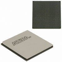
EP3SL150F1152C2N Altera, EP3SL150F1152C2N Datasheet - Page 164

EP3SL150F1152C2N
Manufacturer Part Number
EP3SL150F1152C2N
Description
IC STRATX III FPGA 150K 1152FBGA
Manufacturer
Altera
Series
Stratix® IIIr
Datasheets
1.EP3SL150F780C4N.pdf
(16 pages)
2.EP3SL150F780C4N.pdf
(332 pages)
3.EP3SL150F780C4N.pdf
(456 pages)
Specifications of EP3SL150F1152C2N
Number Of Logic Elements/cells
142500
Number Of Labs/clbs
5700
Total Ram Bits
6390
Number Of I /o
744
Voltage - Supply
0.86 V ~ 1.15 V
Mounting Type
Surface Mount
Operating Temperature
0°C ~ 85°C
Package / Case
1152-FBGA
For Use With
544-2568 - KIT DEVELOPMENT STRATIX III
Lead Free Status / RoHS Status
Lead free / RoHS Compliant
Number Of Gates
-
Other names
544-2409
EP3SL150F1152C2NES
EP3SL150F1152C2NES
Available stocks
Company
Part Number
Manufacturer
Quantity
Price
Part Number:
EP3SL150F1152C2N
Manufacturer:
ALTERA
Quantity:
20 000
- Current page: 164 of 456
- Download datasheet (7Mb)
6–16
Stratix III Device Handbook, Volume 1
Quartus II software. The dynamic clock enable or disable feature allows the internal
logic to control power-up or power-down synchronously on GCLK and RCLK
networks, including dual-regional clock regions. This function is independent of the
PLL and is applied directly on the clock network, as shown in
Figure
You can set the input clock sources and the clkena signals for the global and regional
clock network multiplexers through the Quartus II software using the ALTCLKCTRL
megafunction. You can also enable or disable the dedicated external clock output pins
using the ALTCLKCTRL megafunction.
When using the ALTCLKCTRL megafunction to implement clock source selection
(dynamic), the inputs from the clock pins feed the inclock[0..1] ports of the
multiplexer, while the PLL outputs feed the inclock[2..3] ports. You can choose
from among these inputs using the CLKSELECT[1..0] signal.
Figure 6–15
Figure 6–15. Stratix III External PLL Output Clock Control Block
Notes to
(1) This clock select signal can only be set through a configuration file (.sof or .pof) and cannot be dynamically controlled
(2) The clock control block feeds to a multiplexer within the PLL_<#>_CLKOUT pin's IOE. The PLL_<#>_CLKOUT
during user mode operation.
pin is a dual-purpose pin. Therefore, this multiplexer selects either an internal signal or the output of the clock control
block.
Figure
6–14.
shows the external PLL output clock control block.
6–15:
IOE
Internal
Logic
(2)
PLL_<#>_CLKOUT pin
7 or 10
PLL Counter
Outputs
Enable/
Disable
Chapter 6: Clock Networks and PLLs in Stratix III Devices
Internal
Static Clock
Select (1)
Logic
Static Clock Select
(1)
Clock Networks in Stratix III Devices
© July 2010 Altera Corporation
Figure 6–13
and
Related parts for EP3SL150F1152C2N
Image
Part Number
Description
Manufacturer
Datasheet
Request
R

Part Number:
Description:
CYCLONE II STARTER KIT EP2C20N
Manufacturer:
Altera
Datasheet:

Part Number:
Description:
CPLD, EP610 Family, ECMOS Process, 300 Gates, 16 Macro Cells, 16 Reg., 16 User I/Os, 5V Supply, 35 Speed Grade, 24DIP
Manufacturer:
Altera Corporation
Datasheet:

Part Number:
Description:
CPLD, EP610 Family, ECMOS Process, 300 Gates, 16 Macro Cells, 16 Reg., 16 User I/Os, 5V Supply, 15 Speed Grade, 24DIP
Manufacturer:
Altera Corporation
Datasheet:

Part Number:
Description:
Manufacturer:
Altera Corporation
Datasheet:

Part Number:
Description:
CPLD, EP610 Family, ECMOS Process, 300 Gates, 16 Macro Cells, 16 Reg., 16 User I/Os, 5V Supply, 30 Speed Grade, 24DIP
Manufacturer:
Altera Corporation
Datasheet:

Part Number:
Description:
High-performance, low-power erasable programmable logic devices with 8 macrocells, 10ns
Manufacturer:
Altera Corporation
Datasheet:

Part Number:
Description:
High-performance, low-power erasable programmable logic devices with 8 macrocells, 7ns
Manufacturer:
Altera Corporation
Datasheet:

Part Number:
Description:
Classic EPLD
Manufacturer:
Altera Corporation
Datasheet:

Part Number:
Description:
High-performance, low-power erasable programmable logic devices with 8 macrocells, 10ns
Manufacturer:
Altera Corporation
Datasheet:

Part Number:
Description:
Manufacturer:
Altera Corporation
Datasheet:

Part Number:
Description:
Manufacturer:
Altera Corporation
Datasheet:

Part Number:
Description:
Manufacturer:
Altera Corporation
Datasheet:

Part Number:
Description:
CPLD, EP610 Family, ECMOS Process, 300 Gates, 16 Macro Cells, 16 Reg., 16 User I/Os, 5V Supply, 25 Speed Grade, 24DIP
Manufacturer:
Altera Corporation
Datasheet:


