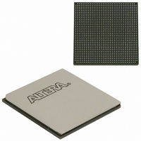
EP3SL150F1152C2N Altera, EP3SL150F1152C2N Datasheet - Page 223

EP3SL150F1152C2N
Manufacturer Part Number
EP3SL150F1152C2N
Description
IC STRATX III FPGA 150K 1152FBGA
Manufacturer
Altera
Series
Stratix® IIIr
Datasheets
1.EP3SL150F780C4N.pdf
(16 pages)
2.EP3SL150F780C4N.pdf
(332 pages)
3.EP3SL150F780C4N.pdf
(456 pages)
Specifications of EP3SL150F1152C2N
Number Of Logic Elements/cells
142500
Number Of Labs/clbs
5700
Total Ram Bits
6390
Number Of I /o
744
Voltage - Supply
0.86 V ~ 1.15 V
Mounting Type
Surface Mount
Operating Temperature
0°C ~ 85°C
Package / Case
1152-FBGA
For Use With
544-2568 - KIT DEVELOPMENT STRATIX III
Lead Free Status / RoHS Status
Lead free / RoHS Compliant
Number Of Gates
-
Other names
544-2409
EP3SL150F1152C2NES
EP3SL150F1152C2NES
Available stocks
Company
Part Number
Manufacturer
Quantity
Price
Part Number:
EP3SL150F1152C2N
Manufacturer:
ALTERA
Quantity:
20 000
- Current page: 223 of 456
- Download datasheet (7Mb)
Chapter 7: Stratix III Device I/O Features
Stratix III I/O Structure
Programmable Differential Output Voltage
MultiVolt I/O Interface
Table 7–7. MultiVolt I/O Support for Stratix III Devices
© July 2010
Notes to
(1) The pin current may be slightly higher than the default value. You must verify that the driving device’s V
(2) Use on-chip PCI clamp diode for column I/Os or external PCI clamp diode for row I/Os to protect the input pins against overshoot voltage.
(3) Each I/O bank of a Stratix III device has its own VCCIO pins and supports only one V
V
CCIO
3.3
1.2
1.5
1.8
2.5
3.0
do not violate the applicable Stratix III V
requires that a V
(V)
Table
Altera Corporation
f
1.2
7–7:
v
—
—
—
—
—
1
CCIO
of 2.5 V cannot be assigned in a same bank with a 3.0-V or 3.3-V output signal.
1.5
—
v
v
—
—
—
Stratix III LVDS transmitters support programmable V
settings enable you to adjust output eye height to optimize for trace length and power
consumption. A higher V
a smaller V
settings for programmable V
default setting is medium low.
For more information about programmable V
Interfaces with DPA in the Stratix III Devices
The Stratix III architecture supports the MultiVolt
Stratix III devices in all packages to interface with systems of different supply
voltages.
You can connect the V
depending on the output requirements. The output levels are compatible with
systems of the same voltage as the power supply. (For example, when V
connected to a 1.5-V power supply, the output levels are compatible with 1.5-V
systems.)
You must connect the Stratix III VCCPD power pins to a 2.5-, 3.0 or 3.3-V power supply.
Using these power pins to supply the pre-driver power to the output buffers increases
the performance of the output pins.
support.
For V
V
CCPD
CCIO
= 2.5 V.
v
Input Signal (V)
1.8
—
v
—
—
—
= 3.3 V, V
(1)
OD
IL
swing reduces power consumption. The Quartus II software allows four
maximum and V
2.5
v
v
v
—
—
—
CCPD
CCIO
=3.3 V. For V
v
3.0
v
v
—
—
—
OD
IH
pins to a 1.2-, 1.5-, 1.8-, 2.5-, 3.0 or 3.3-V power supply,
(2)
minimum voltage specifications.
swing improves voltage margins at the receiver end while
(Note
OD
—low, medium low, medium high, and high. The
v
3.3
—
—
—
v
v
1),
(2)
CCIO
(2)
Table 7–7
= 3.0 V, V
1.2
v
—
—
—
—
—
chapter.
ccio
OD
summarizes Stratix III MultiVolt I/O
, either 1.2, 1.5, 1.8, or 3.0 V. The LVDS I/O standard
, refer to the
CCPD
1.5
TM
v
—
—
—
—
—
I/O interface feature that allows
= 3.0 V. For V
OD
Output Signal (V)
OL
. The programmable V
maximum and V
1.8
—
—
v
—
—
—
Stratix III Device Handbook, Volume 1
High Speed Differential I/O
CCIO
2.5
v
—
—
—
—
—
OH
= 2.5 V or less,
minimum voltages
CCIO
3.0
—
—
—
—
v
—
pins are
OD
3.3
—
—
—
—
—
v
7–19
Related parts for EP3SL150F1152C2N
Image
Part Number
Description
Manufacturer
Datasheet
Request
R

Part Number:
Description:
CYCLONE II STARTER KIT EP2C20N
Manufacturer:
Altera
Datasheet:

Part Number:
Description:
CPLD, EP610 Family, ECMOS Process, 300 Gates, 16 Macro Cells, 16 Reg., 16 User I/Os, 5V Supply, 35 Speed Grade, 24DIP
Manufacturer:
Altera Corporation
Datasheet:

Part Number:
Description:
CPLD, EP610 Family, ECMOS Process, 300 Gates, 16 Macro Cells, 16 Reg., 16 User I/Os, 5V Supply, 15 Speed Grade, 24DIP
Manufacturer:
Altera Corporation
Datasheet:

Part Number:
Description:
Manufacturer:
Altera Corporation
Datasheet:

Part Number:
Description:
CPLD, EP610 Family, ECMOS Process, 300 Gates, 16 Macro Cells, 16 Reg., 16 User I/Os, 5V Supply, 30 Speed Grade, 24DIP
Manufacturer:
Altera Corporation
Datasheet:

Part Number:
Description:
High-performance, low-power erasable programmable logic devices with 8 macrocells, 10ns
Manufacturer:
Altera Corporation
Datasheet:

Part Number:
Description:
High-performance, low-power erasable programmable logic devices with 8 macrocells, 7ns
Manufacturer:
Altera Corporation
Datasheet:

Part Number:
Description:
Classic EPLD
Manufacturer:
Altera Corporation
Datasheet:

Part Number:
Description:
High-performance, low-power erasable programmable logic devices with 8 macrocells, 10ns
Manufacturer:
Altera Corporation
Datasheet:

Part Number:
Description:
Manufacturer:
Altera Corporation
Datasheet:

Part Number:
Description:
Manufacturer:
Altera Corporation
Datasheet:

Part Number:
Description:
Manufacturer:
Altera Corporation
Datasheet:

Part Number:
Description:
CPLD, EP610 Family, ECMOS Process, 300 Gates, 16 Macro Cells, 16 Reg., 16 User I/Os, 5V Supply, 25 Speed Grade, 24DIP
Manufacturer:
Altera Corporation
Datasheet:


