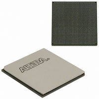
EP3SL150F1152C2N Altera, EP3SL150F1152C2N Datasheet - Page 172

EP3SL150F1152C2N
Manufacturer Part Number
EP3SL150F1152C2N
Description
IC STRATX III FPGA 150K 1152FBGA
Manufacturer
Altera
Series
Stratix® IIIr
Datasheets
1.EP3SL150F780C4N.pdf
(16 pages)
2.EP3SL150F780C4N.pdf
(332 pages)
3.EP3SL150F780C4N.pdf
(456 pages)
Specifications of EP3SL150F1152C2N
Number Of Logic Elements/cells
142500
Number Of Labs/clbs
5700
Total Ram Bits
6390
Number Of I /o
744
Voltage - Supply
0.86 V ~ 1.15 V
Mounting Type
Surface Mount
Operating Temperature
0°C ~ 85°C
Package / Case
1152-FBGA
For Use With
544-2568 - KIT DEVELOPMENT STRATIX III
Lead Free Status / RoHS Status
Lead free / RoHS Compliant
Number Of Gates
-
Other names
544-2409
EP3SL150F1152C2NES
EP3SL150F1152C2NES
Available stocks
Company
Part Number
Manufacturer
Quantity
Price
Part Number:
EP3SL150F1152C2N
Manufacturer:
ALTERA
Quantity:
20 000
- Current page: 172 of 456
- Download datasheet (7Mb)
6–24
Stratix III PLL Software Overview
Figure 6–22. Stratix III PLL Ports
Notes to
(1) You can feed the inclk0 or inclk1 clock input from any one of four dedicated clock pins located on the same side of the device as the PLL.
(2) You can drive to global or regional clock networks or dedicated external clock output pins. n = 6 for Left/Right PLLs and n = 9 for Top/Bottom PLLs.
Table 6–12. PLL Input Signals (Part 1 of 2)
Stratix III Device Handbook, Volume 1
inclk0
inclk1
fbin
clkswitch
Figure
Port
6–22:
Input clock to the PLL
Input clock to the PLL
Compensation feedback input to the
PLL. Share the same clock spines used
by GCLK/RCLKs.
Switchover signal used to initiate clock
switchover asynchronously. When used
in manual switchover, clkswitch is
used as a select signal between
inclk0 and inclk1. If
clkswitch = 0, inclk0 is
selected. If clkswitch = 1, inclk1
is selected. Both inclk0 and inclk1
must be switched in order for manual
switchover to function.
Stratix III PLLs are enabled in the Quartus II software by using the ALTPLL
megafunction.
ALTPLL megafunction of the Quartus II software.
Table 6–12
inclk0 (1)
inclk1 (1)
fbin
clkswitch
areset
pfdena
scanclk
scandata
scanclkena
configupdate
phasecounterselect[3..0]
phaseupdown
phasestep
Description
lists the PLL input signals for Stratix III devices.
Figure 6–22
shows the Stratix III PLL ports as they are named in the
scandataout
clkbad[1..0]
(2) clk[n..0]
phasedone
activeclock
scandone
locked
fbout
Dedicated pin, adjacent
Dedicated pin, adjacent
Logic array or I/O pin
PLL, GCLK, or RCLK
PLL, GCLK, or RCLK
Pin LVSDCLK
Chapter 6: Clock Networks and PLLs in Stratix III Devices
network
network
Source
Signal Driven by Internal Logic
internal logic or I/O pins
Internal Clock Signal
Signal driven to
Physical Pin
© July 2010 Altera Corporation
Clock switchover circuit
PLLs in Stratix III Devices
Destination
N counter
N counter
PFD
Related parts for EP3SL150F1152C2N
Image
Part Number
Description
Manufacturer
Datasheet
Request
R

Part Number:
Description:
CYCLONE II STARTER KIT EP2C20N
Manufacturer:
Altera
Datasheet:

Part Number:
Description:
CPLD, EP610 Family, ECMOS Process, 300 Gates, 16 Macro Cells, 16 Reg., 16 User I/Os, 5V Supply, 35 Speed Grade, 24DIP
Manufacturer:
Altera Corporation
Datasheet:

Part Number:
Description:
CPLD, EP610 Family, ECMOS Process, 300 Gates, 16 Macro Cells, 16 Reg., 16 User I/Os, 5V Supply, 15 Speed Grade, 24DIP
Manufacturer:
Altera Corporation
Datasheet:

Part Number:
Description:
Manufacturer:
Altera Corporation
Datasheet:

Part Number:
Description:
CPLD, EP610 Family, ECMOS Process, 300 Gates, 16 Macro Cells, 16 Reg., 16 User I/Os, 5V Supply, 30 Speed Grade, 24DIP
Manufacturer:
Altera Corporation
Datasheet:

Part Number:
Description:
High-performance, low-power erasable programmable logic devices with 8 macrocells, 10ns
Manufacturer:
Altera Corporation
Datasheet:

Part Number:
Description:
High-performance, low-power erasable programmable logic devices with 8 macrocells, 7ns
Manufacturer:
Altera Corporation
Datasheet:

Part Number:
Description:
Classic EPLD
Manufacturer:
Altera Corporation
Datasheet:

Part Number:
Description:
High-performance, low-power erasable programmable logic devices with 8 macrocells, 10ns
Manufacturer:
Altera Corporation
Datasheet:

Part Number:
Description:
Manufacturer:
Altera Corporation
Datasheet:

Part Number:
Description:
Manufacturer:
Altera Corporation
Datasheet:

Part Number:
Description:
Manufacturer:
Altera Corporation
Datasheet:

Part Number:
Description:
CPLD, EP610 Family, ECMOS Process, 300 Gates, 16 Macro Cells, 16 Reg., 16 User I/Os, 5V Supply, 25 Speed Grade, 24DIP
Manufacturer:
Altera Corporation
Datasheet:


