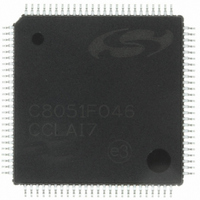
C8051F046-GQ Silicon Laboratories Inc, C8051F046-GQ Datasheet - Page 106

C8051F046-GQ
Manufacturer Part Number
C8051F046-GQ
Description
IC 8051 MCU 32K FLASH 100TQFP
Manufacturer
Silicon Laboratories Inc
Series
C8051F04xr
Specifications of C8051F046-GQ
Core Processor
8051
Core Size
8-Bit
Speed
25MHz
Connectivity
CAN, EBI/EMI, SMBus (2-Wire/I²C), SPI, UART/USART
Peripherals
Brown-out Detect/Reset, POR, PWM, Temp Sensor, WDT
Number Of I /o
64
Program Memory Size
32KB (32K x 8)
Program Memory Type
FLASH
Ram Size
4.25K x 8
Voltage - Supply (vcc/vdd)
2.7 V ~ 3.6 V
Data Converters
A/D 13x10b
Oscillator Type
Internal
Operating Temperature
-40°C ~ 85°C
Package / Case
100-TQFP, 100-VQFP
Processor Series
C8051F0x
Core
8051
Data Bus Width
8 bit
Data Ram Size
4.25 KB
Interface Type
CAN, SMBus, SPI, UART
Maximum Clock Frequency
25 MHz
Number Of Programmable I/os
64
Number Of Timers
5
Operating Supply Voltage
2.7 V to 3.6 V
Maximum Operating Temperature
+ 85 C
Mounting Style
SMD/SMT
3rd Party Development Tools
PK51, CA51, A51, ULINK2
Development Tools By Supplier
C8051F040DK
Minimum Operating Temperature
- 40 C
On-chip Adc
10 bit, 13 Channel
On-chip Dac
12 bit, 2 Channel
Package
100TQFP
Device Core
8051
Family Name
C8051F04x
Maximum Speed
25 MHz
Lead Free Status / RoHS Status
Lead free / RoHS Compliant
Eeprom Size
-
Lead Free Status / Rohs Status
Details
Other names
336-1211
Available stocks
Company
Part Number
Manufacturer
Quantity
Price
Company:
Part Number:
C8051F046-GQ
Manufacturer:
Silicon Laboratories Inc
Quantity:
10 000
Company:
Part Number:
C8051F046-GQR
Manufacturer:
AMAZING
Quantity:
67 000
Company:
Part Number:
C8051F046-GQR
Manufacturer:
Silicon Laboratories Inc
Quantity:
10 000
- Current page: 106 of 328
- Download datasheet (3Mb)
C8051F040/1/2/3/4/5/6/7
8.1.
Each DAC features a flexible output update mechanism which allows for seamless full-scale changes and
supports jitter-free updates for waveform generation. The following examples are written in terms of DAC0,
but DAC1 operation is identical.
8.1.1. Update Output On-Demand
In its default mode (DAC0CN.[4:3] = ‘00’) the DAC0 output is updated “on-demand” on a write to the high-
byte of the DAC0 data register (DAC0H). It is important to note that writes to DAC0L are held, and have no
effect on the DAC0 output until a write to DAC0H takes place. If writing a full 12-bit word to the DAC data
registers, the 12-bit data word is written to the low byte (DAC0L) and high byte (DAC0H) data registers.
Data is latched into DAC0 after a write to the corresponding DAC0H register, so the write sequence
should be DAC0L followed by DAC0H if the full 12-bit resolution is required. The DAC can be used in 8-
bit mode by initializing DAC0L to the desired value (typically 0x00), and writing data to only DAC0H (also
see
8.1.2. Update Output Based on Timer Overflow
Similar to the ADC operation, in which an ADC conversion can be initiated by a timer overflow indepen-
dently of the processor, the DAC outputs can use a Timer overflow to schedule an output update event.
This feature is useful in systems where the DAC is used to generate a waveform of a defined sampling rate
by eliminating the effects of variable interrupt latency and instruction execution on the timing of the DAC
output. When the DAC0MD bits (DAC0CN.[4:3]) are set to ‘01’, ‘10’, or ‘11’, writes to both DAC data regis-
ters (DAC0L and DAC0H) are held until an associated Timer overflow event (Timer 3, Timer 4, or Timer 2,
respectively) occurs, at which time the DAC0H:DAC0L contents are copied to the DAC input latches allow-
ing the DAC output to change to the new value.
8.2.
In some instances, input data should be shifted prior to a DAC0 write operation to properly justify data
within the DAC input registers. This action would typically require one or more load and shift operations,
adding software overhead and slowing DAC throughput. To alleviate this problem, the data-formatting fea-
ture provides a means for the user to program the orientation of the DAC0 data word within data registers
DAC0H and DAC0L. The three DAC0DF bits (DAC0CN.[2:0]) allow the user to specify one of five data
word orientations as shown in the DAC0CN register definition.
DAC1 is functionally the same as DAC0 described above. The electrical specifications for both DAC0 and
DAC1 are given in Table 8.1.
106
Section 8.2
DAC Output Scheduling
DAC Output Scaling/Justification
for information on formatting the 12-bit DAC data word within the 16-bit SFR space).
Rev. 1.5
Related parts for C8051F046-GQ
Image
Part Number
Description
Manufacturer
Datasheet
Request
R
Part Number:
Description:
SMD/C°/SINGLE-ENDED OUTPUT SILICON OSCILLATOR
Manufacturer:
Silicon Laboratories Inc
Part Number:
Description:
Manufacturer:
Silicon Laboratories Inc
Datasheet:
Part Number:
Description:
N/A N/A/SI4010 AES KEYFOB DEMO WITH LCD RX
Manufacturer:
Silicon Laboratories Inc
Datasheet:
Part Number:
Description:
N/A N/A/SI4010 SIMPLIFIED KEY FOB DEMO WITH LED RX
Manufacturer:
Silicon Laboratories Inc
Datasheet:
Part Number:
Description:
N/A/-40 TO 85 OC/EZLINK MODULE; F930/4432 HIGH BAND (REV E/B1)
Manufacturer:
Silicon Laboratories Inc
Part Number:
Description:
EZLink Module; F930/4432 Low Band (rev e/B1)
Manufacturer:
Silicon Laboratories Inc
Part Number:
Description:
I°/4460 10 DBM RADIO TEST CARD 434 MHZ
Manufacturer:
Silicon Laboratories Inc
Part Number:
Description:
I°/4461 14 DBM RADIO TEST CARD 868 MHZ
Manufacturer:
Silicon Laboratories Inc
Part Number:
Description:
I°/4463 20 DBM RFSWITCH RADIO TEST CARD 460 MHZ
Manufacturer:
Silicon Laboratories Inc
Part Number:
Description:
I°/4463 20 DBM RADIO TEST CARD 868 MHZ
Manufacturer:
Silicon Laboratories Inc
Part Number:
Description:
I°/4463 27 DBM RADIO TEST CARD 868 MHZ
Manufacturer:
Silicon Laboratories Inc
Part Number:
Description:
I°/4463 SKYWORKS 30 DBM RADIO TEST CARD 915 MHZ
Manufacturer:
Silicon Laboratories Inc
Part Number:
Description:
N/A N/A/-40 TO 85 OC/4463 RFMD 30 DBM RADIO TEST CARD 915 MHZ
Manufacturer:
Silicon Laboratories Inc
Part Number:
Description:
I°/4463 20 DBM RADIO TEST CARD 169 MHZ
Manufacturer:
Silicon Laboratories Inc


