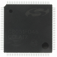
C8051F046-GQ Silicon Laboratories Inc, C8051F046-GQ Datasheet - Page 242

C8051F046-GQ
Manufacturer Part Number
C8051F046-GQ
Description
IC 8051 MCU 32K FLASH 100TQFP
Manufacturer
Silicon Laboratories Inc
Series
C8051F04xr
Specifications of C8051F046-GQ
Core Processor
8051
Core Size
8-Bit
Speed
25MHz
Connectivity
CAN, EBI/EMI, SMBus (2-Wire/I²C), SPI, UART/USART
Peripherals
Brown-out Detect/Reset, POR, PWM, Temp Sensor, WDT
Number Of I /o
64
Program Memory Size
32KB (32K x 8)
Program Memory Type
FLASH
Ram Size
4.25K x 8
Voltage - Supply (vcc/vdd)
2.7 V ~ 3.6 V
Data Converters
A/D 13x10b
Oscillator Type
Internal
Operating Temperature
-40°C ~ 85°C
Package / Case
100-TQFP, 100-VQFP
Processor Series
C8051F0x
Core
8051
Data Bus Width
8 bit
Data Ram Size
4.25 KB
Interface Type
CAN, SMBus, SPI, UART
Maximum Clock Frequency
25 MHz
Number Of Programmable I/os
64
Number Of Timers
5
Operating Supply Voltage
2.7 V to 3.6 V
Maximum Operating Temperature
+ 85 C
Mounting Style
SMD/SMT
3rd Party Development Tools
PK51, CA51, A51, ULINK2
Development Tools By Supplier
C8051F040DK
Minimum Operating Temperature
- 40 C
On-chip Adc
10 bit, 13 Channel
On-chip Dac
12 bit, 2 Channel
Package
100TQFP
Device Core
8051
Family Name
C8051F04x
Maximum Speed
25 MHz
Lead Free Status / RoHS Status
Lead free / RoHS Compliant
Eeprom Size
-
Lead Free Status / Rohs Status
Details
Other names
336-1211
Available stocks
Company
Part Number
Manufacturer
Quantity
Price
Company:
Part Number:
C8051F046-GQ
Manufacturer:
Silicon Laboratories Inc
Quantity:
10 000
Company:
Part Number:
C8051F046-GQR
Manufacturer:
AMAZING
Quantity:
67 000
Company:
Part Number:
C8051F046-GQR
Manufacturer:
Silicon Laboratories Inc
Quantity:
10 000
- Current page: 242 of 328
- Download datasheet (3Mb)
C8051F040/1/2/3/4/5/6/7
19.2.2. Clock Low Extension
SMBus provides a clock synchronization mechanism, similar to I
speed capabilities to coexist on the bus. A clock-low extension is used during a transfer in order to allow
slower slave devices to communicate with faster masters. The slave may temporarily hold the SCL line
LOW to extend the clock low period, effectively decreasing the serial clock frequency.
19.2.3. SCL Low Timeout
If the SCL line is held low by a slave device on the bus, no further communication is possible. Furthermore,
the master cannot force the SCL line high to correct the error condition. To solve this problem, the SMBus
protocol specifies that devices participating in a transfer must detect any clock cycle held low longer than
25 ms as a “timeout” condition. Devices that have detected the timeout condition must reset the communi-
cation no later than 10 ms after detecting the timeout condition.
19.2.4. SCL High (SMBus Free) Timeout
The SMBus specification stipulates that if the SCL and SDA lines remain high for more that 50 µs, the bus
is designated as free. If an SMBus device is waiting to generate a Master START, the START will be gen-
erated following the bus free timeout.
19.3. SMBus Transfer Modes
The SMBus0 interface may be configured to operate as a master and/or a slave. At any particular time, the
interface will be operating in one of the following modes: Master Transmitter, Master Receiver, Slave
Transmitter, or Slave Receiver. See Table 19.1 for transfer mode status decoding using the SMB0STA sta-
tus register. The following mode descriptions illustrate an interrupt-driven SMBus0 application; SMBus0
may alternatively be operated in polled mode.
19.3.1. Master Transmitter Mode
Serial data is transmitted on SDA while the serial clock is output on SCL. SMBus0 generates a START
condition and then transmits the first byte containing the address of the target slave device and the data
direction bit. In this case the data direction bit (R/W) will be logic 0 to indicate a "WRITE" operation. The
SMBus0 interface transmits one or more bytes of serial data, waiting for an acknowledge (ACK) from the
slave after each byte. To indicate the end of the serial transfer, SMBus0 generates a STOP condition.
242
Interrupt
S
Received by SMBus
Interface
Transmitted by
SMBus Interface
Figure 19.4. Typical Master Transmitter Sequence
SLA
W
Interrupt
A
Data Byte
Rev. 1.5
Interrupt
A
2
C, which allows devices with different
S = START
P = STOP
A = ACK
W = WRITE
SLA = Slave Address
Data Byte
Interrupt
A
P
Related parts for C8051F046-GQ
Image
Part Number
Description
Manufacturer
Datasheet
Request
R
Part Number:
Description:
SMD/C°/SINGLE-ENDED OUTPUT SILICON OSCILLATOR
Manufacturer:
Silicon Laboratories Inc
Part Number:
Description:
Manufacturer:
Silicon Laboratories Inc
Datasheet:
Part Number:
Description:
N/A N/A/SI4010 AES KEYFOB DEMO WITH LCD RX
Manufacturer:
Silicon Laboratories Inc
Datasheet:
Part Number:
Description:
N/A N/A/SI4010 SIMPLIFIED KEY FOB DEMO WITH LED RX
Manufacturer:
Silicon Laboratories Inc
Datasheet:
Part Number:
Description:
N/A/-40 TO 85 OC/EZLINK MODULE; F930/4432 HIGH BAND (REV E/B1)
Manufacturer:
Silicon Laboratories Inc
Part Number:
Description:
EZLink Module; F930/4432 Low Band (rev e/B1)
Manufacturer:
Silicon Laboratories Inc
Part Number:
Description:
I°/4460 10 DBM RADIO TEST CARD 434 MHZ
Manufacturer:
Silicon Laboratories Inc
Part Number:
Description:
I°/4461 14 DBM RADIO TEST CARD 868 MHZ
Manufacturer:
Silicon Laboratories Inc
Part Number:
Description:
I°/4463 20 DBM RFSWITCH RADIO TEST CARD 460 MHZ
Manufacturer:
Silicon Laboratories Inc
Part Number:
Description:
I°/4463 20 DBM RADIO TEST CARD 868 MHZ
Manufacturer:
Silicon Laboratories Inc
Part Number:
Description:
I°/4463 27 DBM RADIO TEST CARD 868 MHZ
Manufacturer:
Silicon Laboratories Inc
Part Number:
Description:
I°/4463 SKYWORKS 30 DBM RADIO TEST CARD 915 MHZ
Manufacturer:
Silicon Laboratories Inc
Part Number:
Description:
N/A N/A/-40 TO 85 OC/4463 RFMD 30 DBM RADIO TEST CARD 915 MHZ
Manufacturer:
Silicon Laboratories Inc
Part Number:
Description:
I°/4463 20 DBM RADIO TEST CARD 169 MHZ
Manufacturer:
Silicon Laboratories Inc


