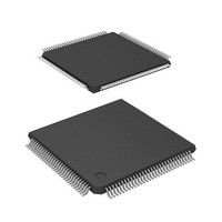
DF2398TE20 Renesas Electronics America, DF2398TE20 Datasheet - Page 47

DF2398TE20
Manufacturer Part Number
DF2398TE20
Description
IC H8S MCU FLASH 256K 120TQFP
Manufacturer
Renesas Electronics America
Series
H8® H8S/2300r
Specifications of DF2398TE20
Core Processor
H8S/2000
Core Size
16-Bit
Speed
20MHz
Connectivity
SCI, SmartCard
Peripherals
DMA, POR, PWM, WDT
Number Of I /o
87
Program Memory Size
256KB (256K x 8)
Program Memory Type
FLASH
Ram Size
8K x 8
Voltage - Supply (vcc/vdd)
4.5 V ~ 5.5 V
Data Converters
A/D 8x10b; D/A 2x8b
Oscillator Type
Internal
Operating Temperature
-20°C ~ 75°C
Package / Case
120-TQFP, 120-VQFP
Lead Free Status / RoHS Status
Contains lead / RoHS non-compliant
Eeprom Size
-
Other names
HD64F2398TE20
HD64F2398TE20
HD64F2398TE20
Available stocks
Company
Part Number
Manufacturer
Quantity
Price
Company:
Part Number:
DF2398TE20V
Manufacturer:
Renesas Electronics America
Quantity:
10 000
- Current page: 47 of 1049
- Download datasheet (5Mb)
Type
Address bus
Data bus
Bus control
DMA controller
(DMAC)
Symbol
A
A
D
D
CS7 to
CS0
AS
RD
HWR
LWR
CAS
WAIT
LCAS
DREQ1,
DREQ0
TEND1,
TEND0
DACK1,
DACK0
23
0
15
0
to
to
TFP-120
28 to 25,
23 to 16,
14 to 7,
5 to 2
51 to 48,
46 to 39,
37 to 34
120 to 117
61, 60,
30, 29
82
83
84
85
116
86
86
62, 60
63, 61
112, 111
Pin No.
FP-128B I/O
32 to 29,
27 to 20,
18 to 11,
9 to 6
57 to 54,
52 to 45,
43 to 40
128, 127,
69, 66,
34, 33,
2, 1
90
91
92
93
126
94
94
70, 66
71, 69
122, 121
Output Address bus: These pins output an
I/O
Output Chip select: Signals for selecting
Output Address strobe: When this pin is
Output Read: When this pin is low, it
Output High write/write enable:
Output Low write:
Output Upper column address
Input
Output Lower column address strobe: The
Input
Output DMA transfer end 1 and 0: These
Output DMA transfer acknowledge 1 and
Name and Function
address.
Data bus: These pins constitute a
bidirectional data bus.
areas 7 to 0.
low, it indicates that address output
on the address bus is enabled.
indicates that the external address
space can be read.
A strobe signal that writes to external
space and indicates that the upper
half (D
enabled.
The 2CAS type DRAM write enable
signal.
A strobe signal that writes to external
space and indicates that the lower
half (D
enabled.
strobe/column address strobe:
The 2CAS type DRAM upper column
address strobe signal.
Wait: Requests insertion of a wait
state in the bus cycle when
accessing external 3-state address
space.
2-CAS type DRAM lower column
address strobe signal
DMA request 1 and 0: These pins
request DMAC activation.
pins indicate the end of DMAC data
transfer.
0: These are the DMAC single
address transfer acknowledge pins.
15
7
to D
to D
Rev.6.00 Oct.28.2004 page 17 of 1016
0
8
) of the data bus is
) of the data bus is
REJ09B0138-0600H
Related parts for DF2398TE20
Image
Part Number
Description
Manufacturer
Datasheet
Request
R

Part Number:
Description:
CONN PLUG 12POS DUAL 0.5MM SMD
Manufacturer:
Hirose Electric Co Ltd
Datasheet:

Part Number:
Description:
CONN PLUG 18POS DUAL 0.5MM SMD
Manufacturer:
Hirose Electric Co Ltd
Datasheet:

Part Number:
Description:
CONN PLUG 14POS DUAL 0.5MM SMD
Manufacturer:
Hirose Electric Co Ltd
Datasheet:

Part Number:
Description:
CONN RECEPT 20POS DUAL 0.5MM SMD
Manufacturer:
Hirose Electric Co Ltd
Datasheet:

Part Number:
Description:
CONN PLUG 16POS DUAL 0.5MM SMD
Manufacturer:
Hirose Electric Co Ltd
Datasheet:

Part Number:
Description:
CONN RECEPT 16POS DUAL 0.5MM SMD
Manufacturer:
Hirose Electric Co Ltd
Datasheet:

Part Number:
Description:
CONN PLUG 20POS DUAL 0.5MM SMD
Manufacturer:
Hirose Electric Co Ltd
Datasheet:

Part Number:
Description:
CONN PLUG 30POS DUAL 0.5MM SMD
Manufacturer:
Hirose Electric Co Ltd
Datasheet:

Part Number:
Description:
CONN RECEPT 30POS DUAL 0.5MM SMD
Manufacturer:
Hirose Electric Co Ltd
Datasheet:

Part Number:
Description:
CONN PLUG 40POS DUAL 0.5MM SMD
Manufacturer:
Hirose Electric Co Ltd
Datasheet:

Part Number:
Description:
KIT STARTER FOR M16C/29
Manufacturer:
Renesas Electronics America
Datasheet:

Part Number:
Description:
KIT STARTER FOR R8C/2D
Manufacturer:
Renesas Electronics America
Datasheet:

Part Number:
Description:
R0K33062P STARTER KIT
Manufacturer:
Renesas Electronics America
Datasheet:

Part Number:
Description:
KIT STARTER FOR R8C/23 E8A
Manufacturer:
Renesas Electronics America
Datasheet:

Part Number:
Description:
KIT STARTER FOR R8C/25
Manufacturer:
Renesas Electronics America
Datasheet:


