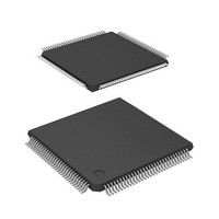
DF2398TE20 Renesas Electronics America, DF2398TE20 Datasheet - Page 840

DF2398TE20
Manufacturer Part Number
DF2398TE20
Description
IC H8S MCU FLASH 256K 120TQFP
Manufacturer
Renesas Electronics America
Series
H8® H8S/2300r
Specifications of DF2398TE20
Core Processor
H8S/2000
Core Size
16-Bit
Speed
20MHz
Connectivity
SCI, SmartCard
Peripherals
DMA, POR, PWM, WDT
Number Of I /o
87
Program Memory Size
256KB (256K x 8)
Program Memory Type
FLASH
Ram Size
8K x 8
Voltage - Supply (vcc/vdd)
4.5 V ~ 5.5 V
Data Converters
A/D 8x10b; D/A 2x8b
Oscillator Type
Internal
Operating Temperature
-20°C ~ 75°C
Package / Case
120-TQFP, 120-VQFP
Lead Free Status / RoHS Status
Contains lead / RoHS non-compliant
Eeprom Size
-
Other names
HD64F2398TE20
HD64F2398TE20
HD64F2398TE20
Available stocks
Company
Part Number
Manufacturer
Quantity
Price
Company:
Part Number:
DF2398TE20V
Manufacturer:
Renesas Electronics America
Quantity:
10 000
- Current page: 840 of 1049
- Download datasheet (5Mb)
A.4
The tables in this section can be used to calculate the number of states required for instruction execution by the CPU.
Table A-5 indicates the number of instruction fetch, data read/write, and other cycles occurring in each instruction. Table
A-4 indicates the number of states required for each cycle. The number of states required for execution of an instruction
can be calculated from these two tables as follows:
Examples: Advanced mode, program code and stack located in external memory, on-chip supporting modules accessed in
two states with 8-bit bus width, external devices accessed in three states with one wait state and 16-bit bus width.
1. BSET #0, @FFFFC7:8
2. JSR @@30
Table A-4
Legend:
m: Number of wait states inserted into external device access
Rev.6.00 Oct.28.2004 page 810 of 1016
REJ09B0138-0600H
From table A-5:
I = L = 2, J = K = M = N = 0
From table A-4:
S
Number of states required for execution = 2
From table A-5:
I = J = K = 2, L = M = N = 0
From table A-4:
S
Number of states required for execution = 2
Execution states = I
I
I
= 4, S
= S
J
Number of States Required for Instruction Execution
= S
Cycle
Instruction fetch
Branch address read S
Stack operation
Byte data access
Word data access
Internal operation
L
Number of States per Cycle
K
= 2
= 4
S
I
+ J S
S
S
S
S
S
I
J
K
L
M
N
J
+ K S
On-Chip
Memory
1
1
K
+ L S
4 + 2 2 = 12
4 + 2 4 + 2 4 = 24
On-Chip Supporting
Module
8-Bit
Bus
4
2
4
1
L
+ M S
16-Bit
Bus
2
1
M
+ N S
Access Conditions
2-State
Access
4
2
4
1
N
8-Bit Bus
3-State
Access
6 + 2m
3 + m
6 + 2m
1
External Device
2-State
Access
2
1
16-Bit Bus
3-State
Access
3 + m
1
Related parts for DF2398TE20
Image
Part Number
Description
Manufacturer
Datasheet
Request
R

Part Number:
Description:
CONN PLUG 12POS DUAL 0.5MM SMD
Manufacturer:
Hirose Electric Co Ltd
Datasheet:

Part Number:
Description:
CONN PLUG 18POS DUAL 0.5MM SMD
Manufacturer:
Hirose Electric Co Ltd
Datasheet:

Part Number:
Description:
CONN PLUG 14POS DUAL 0.5MM SMD
Manufacturer:
Hirose Electric Co Ltd
Datasheet:

Part Number:
Description:
CONN RECEPT 20POS DUAL 0.5MM SMD
Manufacturer:
Hirose Electric Co Ltd
Datasheet:

Part Number:
Description:
CONN PLUG 16POS DUAL 0.5MM SMD
Manufacturer:
Hirose Electric Co Ltd
Datasheet:

Part Number:
Description:
CONN RECEPT 16POS DUAL 0.5MM SMD
Manufacturer:
Hirose Electric Co Ltd
Datasheet:

Part Number:
Description:
CONN PLUG 20POS DUAL 0.5MM SMD
Manufacturer:
Hirose Electric Co Ltd
Datasheet:

Part Number:
Description:
CONN PLUG 30POS DUAL 0.5MM SMD
Manufacturer:
Hirose Electric Co Ltd
Datasheet:

Part Number:
Description:
CONN RECEPT 30POS DUAL 0.5MM SMD
Manufacturer:
Hirose Electric Co Ltd
Datasheet:

Part Number:
Description:
CONN PLUG 40POS DUAL 0.5MM SMD
Manufacturer:
Hirose Electric Co Ltd
Datasheet:

Part Number:
Description:
KIT STARTER FOR M16C/29
Manufacturer:
Renesas Electronics America
Datasheet:

Part Number:
Description:
KIT STARTER FOR R8C/2D
Manufacturer:
Renesas Electronics America
Datasheet:

Part Number:
Description:
R0K33062P STARTER KIT
Manufacturer:
Renesas Electronics America
Datasheet:

Part Number:
Description:
KIT STARTER FOR R8C/23 E8A
Manufacturer:
Renesas Electronics America
Datasheet:

Part Number:
Description:
KIT STARTER FOR R8C/25
Manufacturer:
Renesas Electronics America
Datasheet:


