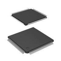
DF2398TE20 Renesas Electronics America, DF2398TE20 Datasheet - Page 677

DF2398TE20
Manufacturer Part Number
DF2398TE20
Description
IC H8S MCU FLASH 256K 120TQFP
Manufacturer
Renesas Electronics America
Series
H8® H8S/2300r
Specifications of DF2398TE20
Core Processor
H8S/2000
Core Size
16-Bit
Speed
20MHz
Connectivity
SCI, SmartCard
Peripherals
DMA, POR, PWM, WDT
Number Of I /o
87
Program Memory Size
256KB (256K x 8)
Program Memory Type
FLASH
Ram Size
8K x 8
Voltage - Supply (vcc/vdd)
4.5 V ~ 5.5 V
Data Converters
A/D 8x10b; D/A 2x8b
Oscillator Type
Internal
Operating Temperature
-20°C ~ 75°C
Package / Case
120-TQFP, 120-VQFP
Lead Free Status / RoHS Status
Contains lead / RoHS non-compliant
Eeprom Size
-
Other names
HD64F2398TE20
HD64F2398TE20
HD64F2398TE20
Available stocks
Company
Part Number
Manufacturer
Quantity
Price
Company:
Part Number:
DF2398TE20V
Manufacturer:
Renesas Electronics America
Quantity:
10 000
- Current page: 677 of 1049
- Download datasheet (5Mb)
19.21
All interrupts, including NMI input, are disabled when flash memory is being programmed or erased (when the P or E bit
is set in FLMCR1), and while the boot program is executing in boot mode*
operation. There are three reasons for this:
1. Interrupt during programming or erasing might cause a violation of the programming or erasing algorithm, with the
2. In the interrupt exception handling sequence during programming or erasing, the vector would not be read correctly*
3. If an interrupt occurred during boot program execution, it would not be possible to execute the normal boot mode
For these reasons, in on-board programming mode alone there are conditions for disabling interrupts, as an exception to
the general rule. However, this provision does not guarantee normal erasing and programming or MCU operation. All
interrupt requests, including NMI, must therefore be restricted inside and outside the MCU when programming or erasing
flash memory. The NMI interrupt is also disabled in the error-protection state while the P or E bit remains set in FLMCR1.
Notes: 1. Interrupt requests must be disabled inside and outside the MCU until the programming control program has
19.22
19.22.1 Programmer Mode Setting
Programs and data can be written and erased in programmer mode as well as in the on-board programming modes. In
programmer mode, the on-chip ROM can be freely programmed using a PROM programmer that supports the Renesas
Technology microcomputer device type with 256-kbyte on-chip flash memory (FZTAT256V5A). Flash memory read
mode, auto-program mode, auto-erase mode, and status read mode are supported with this device type. In auto-program
mode, auto-erase mode, and status read mode, a status polling procedure is used, and in status read mode, detailed internal
signals are output after execution of an auto-program or auto-erase operation.
Table 19-39 shows programmer mode pin settings.
Table 19-39 Programmer Mode Pin Settings
result that normal operation could not be assured.
possibly resulting in MCU runaway.
sequence.
2. The vector may not be read correctly in this case for the following two reasons:
Interrupt Handling when Programming/Erasing Flash Memory
Flash Memory Programmer Mode
completed programming.
•
•
Pin Names
Mode pins: MD2, MD1, MD0
Mode setting pins: P66, P65, P64
STBY pin
RES pin
XTAL, EXTAL pins
Other pins requiring setting: P32, P25
If flash memory is read while being programmed or erased (while the P or E bit is set in FLMCR1), correct
read data will not be obtained (undetermined values will be returned).
If the interrupt entry in the vector table has not been programmed yet, interrupt exception handling will not
be executed correctly.
Settings/External Circuit Connection
Low-level input
High-level input to P66, low-level input to P65 and P64
High-level input (do not select hardware standby mode)
Reset circuit
Oscillator circuit
High-level input to P32, low-level input to P25
1
, to give priority to the program or erase
Rev.6.00 Oct.28.2004 page 647 of 1016
REJ09B0138-0600H
2
,
Related parts for DF2398TE20
Image
Part Number
Description
Manufacturer
Datasheet
Request
R

Part Number:
Description:
CONN PLUG 12POS DUAL 0.5MM SMD
Manufacturer:
Hirose Electric Co Ltd
Datasheet:

Part Number:
Description:
CONN PLUG 18POS DUAL 0.5MM SMD
Manufacturer:
Hirose Electric Co Ltd
Datasheet:

Part Number:
Description:
CONN PLUG 14POS DUAL 0.5MM SMD
Manufacturer:
Hirose Electric Co Ltd
Datasheet:

Part Number:
Description:
CONN RECEPT 20POS DUAL 0.5MM SMD
Manufacturer:
Hirose Electric Co Ltd
Datasheet:

Part Number:
Description:
CONN PLUG 16POS DUAL 0.5MM SMD
Manufacturer:
Hirose Electric Co Ltd
Datasheet:

Part Number:
Description:
CONN RECEPT 16POS DUAL 0.5MM SMD
Manufacturer:
Hirose Electric Co Ltd
Datasheet:

Part Number:
Description:
CONN PLUG 20POS DUAL 0.5MM SMD
Manufacturer:
Hirose Electric Co Ltd
Datasheet:

Part Number:
Description:
CONN PLUG 30POS DUAL 0.5MM SMD
Manufacturer:
Hirose Electric Co Ltd
Datasheet:

Part Number:
Description:
CONN RECEPT 30POS DUAL 0.5MM SMD
Manufacturer:
Hirose Electric Co Ltd
Datasheet:

Part Number:
Description:
CONN PLUG 40POS DUAL 0.5MM SMD
Manufacturer:
Hirose Electric Co Ltd
Datasheet:

Part Number:
Description:
KIT STARTER FOR M16C/29
Manufacturer:
Renesas Electronics America
Datasheet:

Part Number:
Description:
KIT STARTER FOR R8C/2D
Manufacturer:
Renesas Electronics America
Datasheet:

Part Number:
Description:
R0K33062P STARTER KIT
Manufacturer:
Renesas Electronics America
Datasheet:

Part Number:
Description:
KIT STARTER FOR R8C/23 E8A
Manufacturer:
Renesas Electronics America
Datasheet:

Part Number:
Description:
KIT STARTER FOR R8C/25
Manufacturer:
Renesas Electronics America
Datasheet:


