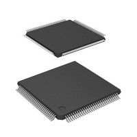
DF2398TE20 Renesas Electronics America, DF2398TE20 Datasheet - Page 626

DF2398TE20
Manufacturer Part Number
DF2398TE20
Description
IC H8S MCU FLASH 256K 120TQFP
Manufacturer
Renesas Electronics America
Series
H8® H8S/2300r
Specifications of DF2398TE20
Core Processor
H8S/2000
Core Size
16-Bit
Speed
20MHz
Connectivity
SCI, SmartCard
Peripherals
DMA, POR, PWM, WDT
Number Of I /o
87
Program Memory Size
256KB (256K x 8)
Program Memory Type
FLASH
Ram Size
8K x 8
Voltage - Supply (vcc/vdd)
4.5 V ~ 5.5 V
Data Converters
A/D 8x10b; D/A 2x8b
Oscillator Type
Internal
Operating Temperature
-20°C ~ 75°C
Package / Case
120-TQFP, 120-VQFP
Lead Free Status / RoHS Status
Contains lead / RoHS non-compliant
Eeprom Size
-
Other names
HD64F2398TE20
HD64F2398TE20
HD64F2398TE20
Available stocks
Company
Part Number
Manufacturer
Quantity
Price
Company:
Part Number:
DF2398TE20V
Manufacturer:
Renesas Electronics America
Quantity:
10 000
- Current page: 626 of 1049
- Download datasheet (5Mb)
19.9.3
Flash memory erasing should be performed block by block following the procedure shown in the erase/erase-verify
flowchart (single-block erase) shown in figure 19-20.
The wait times (x, y, z, , ß,
FLMCR2) and the maximum number of programming operations (N) are shown in table 22.42 in section 22.7.6, Flash
Memory Characteristics.
To perform data or program erasure, make a 1 bit setting for the flash memory area to be erased in erase block register 1 or
2 (EBR1 or EBR2) at least (x) s after setting the SWE bit to 1 in flash memory control register 1 (FLMCR1). Next, the
watchdog timer is set to prevent overerasing in the event of program runaway, etc. Set a value greater than (y + z +
FLMCR2, and after the elapse of (y) s or more, the operating mode is switched to erase mode by setting the E bit in
FLMCR1. The time during which the E bit is set is the flash memory erase time. Ensure that the erase time does not
exceed (z) ms.
Note: With flash memory erasing, preprogramming (setting all data in the memory to be erased to 0) is not necessary
19.9.4
In erase-verify mode, data is read after memory has been erased to check whether it has been correctly erased.
After the elapse of the erase time, erase mode is exited (the E bit in FLMCR1 is cleared to 0, then the ESU bit in FLMCR2
is cleared to 0 at least ( ) s later), the watchdog timer is cleared after the elapse of ( ) s or more, and the operating
mode is switched to erase-verify mode by setting the EV bit in FLMCR1. Before reading in erase-verify mode, a dummy
write of H'FF data should be made to the addresses to be read. The dummy write should be executed after the elapse of ( )
is read. Wait at least ( ) s after the dummy write before performing this read operation. If the read data has been erased
(all 1), a dummy write is performed to the next address, and erase-verify is performed. If the read data has not been erased,
set erase mode again, and repeat the erase/erase-verify sequence in the same way. However, ensure that the erase/erase-
verify sequence is not repeated more than (N) times. When verification is completed, exit erase-verify mode, and wait for
at least ( ) s. If erasure has been completed on all the erase blocks, clear the SWE bit in FLMCR1 to 0. If there are any
unerased blocks, make a 1 bit setting in EBR1 or EBR2 for the flash memory area to be erased, and repeat the erase/erase-
verify sequence in the same way.
Rev.6.00 Oct.28.2004 page 596 of 1016
REJ09B0138-0600H
s as the WDT overflow period. After this, preparation for erase mode (erase setup) is carried out by setting the ESU bit in
s or more. When the flash memory is read in this state (verify data is read in 16-bit units), the data at the latched address
before starting the erase procedure.
Erase Mode
Erase-Verify Mode
after bits are set or cleared in flash memory control registers 1 and 2 (FLMCR1,
+ ß)
Related parts for DF2398TE20
Image
Part Number
Description
Manufacturer
Datasheet
Request
R

Part Number:
Description:
CONN PLUG 12POS DUAL 0.5MM SMD
Manufacturer:
Hirose Electric Co Ltd
Datasheet:

Part Number:
Description:
CONN PLUG 18POS DUAL 0.5MM SMD
Manufacturer:
Hirose Electric Co Ltd
Datasheet:

Part Number:
Description:
CONN PLUG 14POS DUAL 0.5MM SMD
Manufacturer:
Hirose Electric Co Ltd
Datasheet:

Part Number:
Description:
CONN RECEPT 20POS DUAL 0.5MM SMD
Manufacturer:
Hirose Electric Co Ltd
Datasheet:

Part Number:
Description:
CONN PLUG 16POS DUAL 0.5MM SMD
Manufacturer:
Hirose Electric Co Ltd
Datasheet:

Part Number:
Description:
CONN RECEPT 16POS DUAL 0.5MM SMD
Manufacturer:
Hirose Electric Co Ltd
Datasheet:

Part Number:
Description:
CONN PLUG 20POS DUAL 0.5MM SMD
Manufacturer:
Hirose Electric Co Ltd
Datasheet:

Part Number:
Description:
CONN PLUG 30POS DUAL 0.5MM SMD
Manufacturer:
Hirose Electric Co Ltd
Datasheet:

Part Number:
Description:
CONN RECEPT 30POS DUAL 0.5MM SMD
Manufacturer:
Hirose Electric Co Ltd
Datasheet:

Part Number:
Description:
CONN PLUG 40POS DUAL 0.5MM SMD
Manufacturer:
Hirose Electric Co Ltd
Datasheet:

Part Number:
Description:
KIT STARTER FOR M16C/29
Manufacturer:
Renesas Electronics America
Datasheet:

Part Number:
Description:
KIT STARTER FOR R8C/2D
Manufacturer:
Renesas Electronics America
Datasheet:

Part Number:
Description:
R0K33062P STARTER KIT
Manufacturer:
Renesas Electronics America
Datasheet:

Part Number:
Description:
KIT STARTER FOR R8C/23 E8A
Manufacturer:
Renesas Electronics America
Datasheet:

Part Number:
Description:
KIT STARTER FOR R8C/25
Manufacturer:
Renesas Electronics America
Datasheet:


