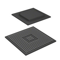
R8A77850ADBGV#RD0Z Renesas Electronics America, R8A77850ADBGV#RD0Z Datasheet - Page 1059

R8A77850ADBGV#RD0Z
Manufacturer Part Number
R8A77850ADBGV#RD0Z
Description
IC SUPERH MPU ROMLESS 436-BGA
Manufacturer
Renesas Electronics America
Series
SuperH® SH7780r
Datasheet
1.R8A77850AADBGV.pdf
(1694 pages)
Specifications of R8A77850ADBGV#RD0Z
Core Processor
SH-4A
Core Size
32-Bit
Speed
600MHz
Connectivity
Audio Codec, MMC, Serial Sound, SCI, SIO, SPI, SSI
Peripherals
DMA, POR, WDT
Number Of I /o
108
Program Memory Type
ROMless
Ram Size
8K x 8
Voltage - Supply (vcc/vdd)
1 V ~ 1.2 V
Oscillator Type
External
Operating Temperature
-40°C ~ 85°C
Package / Case
436-BGA
Lead Free Status / RoHS Status
Lead free / RoHS Compliant
Eeprom Size
-
Program Memory Size
-
Data Converters
-
Available stocks
Company
Part Number
Manufacturer
Quantity
Price
Part Number:
R8A77850ADBGV#RD0ZR8A77850ADBGV
Manufacturer:
Renesas Electronics America
Quantity:
10 000
- Current page: 1059 of 1694
- Download datasheet (9Mb)
(2)
The CPU performs required initialization and starts the processing. IDCT data must be prepared in
the buffer RAM 1. The procedure is shown below.
No. Operation
(7) IDCT data
(8) Estimated
(9) Estimated
reading
image data
generation
image data
writing
MC Processing Procedure
Description
IDCT data stored in buffer RAM 1 is read.
(Only blocks specified by a CBP setting of 1 are read from buffer RAM 1.)
The IDCT data should be stored in buffer RAM 1 as 16-bit signed data.
(The sign is discriminated using the uppermost bit (bit 15).)
Regardless of the CBP value, the IDCT data should be stored in successive
addresses in the order Y0 (128 bytes), Y1 (128 bytes), Y2 (128 bytes), Y3
(128 bytes), U (128 bytes), V (128 bytes).
When there is a CBP=0 block, the address space should not be packed, but
data should be stored in successive addresses in the Y0, Y1, Y2, Y3, U, V
data format.
The CBP value indicates whether a sign is required compared with the
comparison image for the six blocks (four luminance blocks and two
chrominance blocks). The above Y0, Y1, Y2, Y3, U, V are CBP values of
block positions in the following format.
CBP Blocks with YUV4:2:0
(Data for a CBP=0 block: data invalid)
9-bit saturation computation is performed for IDCT data read from RAM 1 (-
256 ≤ x ≤ 255).
(The sign is discriminated using the uppermost bit (bit 15).)
IDCT data reading is performed in parallel with the operation of (5) and (6).
Estimated image data is generated using the following formula from the half-
pixel processing data generated in (6) and the IDCT data (9-bit data after
saturation computation) read in (7).
Formula: (data of (6) + data of (7)) -> (saturation computation) (0 ≤ x ≤ 255)
Estimated image data is written to DDR2-SDRAM at the address computed in
(1) and (2).
Luminance Y
Y0
Y2
20. Graphics Data Translation Accelerator (GDTA)
Y1
Y3
Rev.1.00 Jan. 10, 2008 Page 1027 of 1658
Chrominance
U/V
REJ09B0261-0100
U
V
Related parts for R8A77850ADBGV#RD0Z
Image
Part Number
Description
Manufacturer
Datasheet
Request
R

Part Number:
Description:
KIT STARTER FOR M16C/29
Manufacturer:
Renesas Electronics America
Datasheet:

Part Number:
Description:
KIT STARTER FOR R8C/2D
Manufacturer:
Renesas Electronics America
Datasheet:

Part Number:
Description:
R0K33062P STARTER KIT
Manufacturer:
Renesas Electronics America
Datasheet:

Part Number:
Description:
KIT STARTER FOR R8C/23 E8A
Manufacturer:
Renesas Electronics America
Datasheet:

Part Number:
Description:
KIT STARTER FOR R8C/25
Manufacturer:
Renesas Electronics America
Datasheet:

Part Number:
Description:
KIT STARTER H8S2456 SHARPE DSPLY
Manufacturer:
Renesas Electronics America
Datasheet:

Part Number:
Description:
KIT STARTER FOR R8C38C
Manufacturer:
Renesas Electronics America
Datasheet:

Part Number:
Description:
KIT STARTER FOR R8C35C
Manufacturer:
Renesas Electronics America
Datasheet:

Part Number:
Description:
KIT STARTER FOR R8CL3AC+LCD APPS
Manufacturer:
Renesas Electronics America
Datasheet:

Part Number:
Description:
KIT STARTER FOR RX610
Manufacturer:
Renesas Electronics America
Datasheet:

Part Number:
Description:
KIT STARTER FOR R32C/118
Manufacturer:
Renesas Electronics America
Datasheet:

Part Number:
Description:
KIT DEV RSK-R8C/26-29
Manufacturer:
Renesas Electronics America
Datasheet:

Part Number:
Description:
KIT STARTER FOR SH7124
Manufacturer:
Renesas Electronics America
Datasheet:

Part Number:
Description:
KIT STARTER FOR H8SX/1622
Manufacturer:
Renesas Electronics America
Datasheet:

Part Number:
Description:
KIT DEV FOR SH7203
Manufacturer:
Renesas Electronics America
Datasheet:


