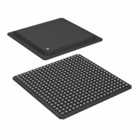
ADSP-21160NCB-100 Analog Devices Inc, ADSP-21160NCB-100 Datasheet - Page 10

ADSP-21160NCB-100
Manufacturer Part Number
ADSP-21160NCB-100
Description
IC,DSP,32-BIT,CMOS,BGA,400PIN,PLASTIC
Manufacturer
Analog Devices Inc
Series
SHARC®r
Type
Floating Pointr
Specifications of ADSP-21160NCB-100
Rohs Status
RoHS non-compliant
Interface
Host Interface, Link Port, Serial Port
Clock Rate
100MHz
Non-volatile Memory
External
On-chip Ram
512kB
Voltage - I/o
3.30V
Voltage - Core
1.90V
Operating Temperature
-40°C ~ 100°C
Mounting Type
Surface Mount
Package / Case
400-BGA
Package
400BGA
Numeric And Arithmetic Format
Floating-Point
Maximum Speed
100 MHz
Ram Size
512 KB
Device Million Instructions Per Second
100 MIPS
Lead Free Status / RoHS Status
Available stocks
Company
Part Number
Manufacturer
Quantity
Price
Company:
Part Number:
ADSP-21160NCB-100
Manufacturer:
Analog Devices Inc
Quantity:
10 000
ADSP-21160N
Tie or pull unused inputs to V
following:
Table 2. Pin Function Descriptions
Pin
ADDR31–0
DATA63–0
MS3–0
RDL
RDH
WRL
WRH
ADDR31–0, DATA63–0, PAGE, BRST, CLKOUT
(ID2–0 = 00x) (Note: These pins have a logic-level hold
circuit enabled on the ADSP-21160N DSP with ID2–0
= 00x.)
PA, ACK, MS3–0, RDx, WRx, CIF, DMARx, DMAGx
(ID2–0 = 00x) (Note: These pins have a pull-up enabled
on the ADSP-21160N DSP with ID2–0 = 00x.)
Type
I/O/T
I/O/T
O/T
I/O/T
I/O/T
I/O/T
I/O/T
DD
or GND, except for the
peripherals on these pins. In a multiprocessor system, the bus master outputs addresses
for read/writes of the internal memory or IOP registers of other ADSP-21160Ns. The
ADSP-21160N inputs addresses when a host processor or multiprocessing bus master
is reading or writing its internal memory or IOP registers. A keeper latch on the DSP’s
ADDR31–0 pins maintains the input at the level it was last driven (only enabled on the
ADSP-21160N with ID2–0 = 00x).
External Bus Data. The ADSP-21160N inputs and outputs data and instructions on
these pins. Pull-up resistors on unused DATA pins are not necessary. A keeper latch on
the DSP’s DATA63-0 pins maintains the input at the level it was last driven (only enabled
on the ADSP-21160N with ID2–0 = 00x).
Memory Select Lines. These outputs are asserted (low) as chip selects for the corre-
sponding banks of external memory. Memory bank size must be defined in the SYSCON
control register. The MS3–0 outputs are decoded memory address lines. In asyn-
chronous access mode, the MS3–0 outputs transition with the other address outputs.
In synchronous access modes, the MS3–0 outputs assert with the other address lines;
however, they deassert after the first CLKIN cycle in which ACK is sampled asserted.
MS3–0 has a 20 k internal pull-up resistor that is enabled on the ADSP-21160N with
ID2–0 = 00x.
low word of external memory or from the internal memory of other ADSP-21160Ns.
External devices, including other ADSP-21160Ns, must assert RDL for reading from
the low word of ADSP-21160N internal memory. In a multiprocessing system, RDL is
driven by the bus master. RDL has a 20 k internal pull-up resistor that is enabled on
the ADSP-21160N with ID2–0 = 00x.
high word of external memory or from the internal memory of other ADSP-21160Ns.
External devices, including other ADSP-21160Ns, must assert RDH for reading from
the high word of ADSP-21160N internal memory. In a multiprocessing system, RDH
is driven by the bus master. RDH has a 20 k internal pull-up resistor that is enabled
on the ADSP-21160N with ID2–0 = 00x.
Memory Write Low Strobe. WRL is asserted when ADSP-21160N writes to the low
word of external memory or internal memory of other ADSP-21160Ns. External devices
must assert WRL for writing to ADSP-21160N’s low word of internal memory. In a
multiprocessing system, WRL is driven by the bus master. WRL has a 20 k internal
pull-up resistor that is enabled on the ADSP-21160N with ID2–0 = 00x.
Memory Write High Strobe. WRH is asserted when ADSP-21160N writes to the high
word of external memory or internal memory of other ADSP-21160Ns. External devices
must assert WRH for writing to ADSP-21160N’s high word of internal memory. In a
multiprocessing system, WRH is driven by the bus master. WRH has a 20 k internal
pull-up resistor that is enabled on the ADSP-21160N with ID2–0 = 00x.
Function
External Bus Address. The ADSP-21160N outputs addresses for external memory and
Memory Read Low Strobe. RDL is asserted whenever ADSP-21160N reads from the
Memory Read High Strobe. RDH is asserted whenever ADSP-21160N reads from the
–10–
The following symbols appear in the Type column of
A = Asynchronous, G = Ground, I = Input, O = Output,
P = Power Supply, S = Synchronous, (A/D) = Active Drive,
(O/D) = Open Drain, and T = Three-State (when SBTS is
asserted, or when the ADSP-21160N is a bus slave).
LxCLK, LxACK, LxDAT7–0 (LxPDRDE = 0) (Note:
See Link Port Buffer Control Register Bit definitions in
the ADSP-21160 DSP Hardware Reference.)
DTx, DRx, TCLKx, RCLKx, EMU, TMS, TRST, TDI
(Note: These pins have a pull-up.)
Table
REV. 0
2:


