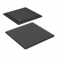
ADSP-21160NCB-100 Analog Devices Inc, ADSP-21160NCB-100 Datasheet - Page 15

ADSP-21160NCB-100
Manufacturer Part Number
ADSP-21160NCB-100
Description
IC,DSP,32-BIT,CMOS,BGA,400PIN,PLASTIC
Manufacturer
Analog Devices Inc
Series
SHARC®r
Type
Floating Pointr
Specifications of ADSP-21160NCB-100
Rohs Status
RoHS non-compliant
Interface
Host Interface, Link Port, Serial Port
Clock Rate
100MHz
Non-volatile Memory
External
On-chip Ram
512kB
Voltage - I/o
3.30V
Voltage - Core
1.90V
Operating Temperature
-40°C ~ 100°C
Mounting Type
Surface Mount
Package / Case
400-BGA
Package
400BGA
Numeric And Arithmetic Format
Floating-Point
Maximum Speed
100 MHz
Ram Size
512 KB
Device Million Instructions Per Second
100 MIPS
Lead Free Status / RoHS Status
Available stocks
Company
Part Number
Manufacturer
Quantity
Price
Company:
Part Number:
ADSP-21160NCB-100
Manufacturer:
Analog Devices Inc
Quantity:
10 000
6
7
8
9
10
11
12
13
14
15
16
17
18
19
20
ABSOLUTE MAXIMUM RATINGS
1
ESD SENSITIVITY
CAUTION
ESD (electrostatic discharge) sensitive device. Electrostatic charges as high as 4000 V
readily accumulate on the human body and test equipment and can discharge without
detection. Although the ADSP-21160N features proprietary ESD protection circuitry,
permanent damage may occur on devices subjected to high energy electrostatic
discharges. Therefore, proper ESD precautions are recommended to avoid performance
degradation or loss of functionality.
REV. 0
Applies to CLKIN only.
Applies to all pins with keeper latches: ADDR31–0, DATA63–0, PAGE, BRST, CLKOUT.
Current required to switch from kept high to low or from kept low to high.
Characterized, but not tested.
Internal (Core) Supply Voltage (V
Analog (PLL) Supply Voltage (AV
External (I/O) Supply Voltage (V
Input Voltage
Output Voltage Swing
Load Capacitance
Storage Temperature Range
Stresses greater than those listed above may cause permanent damage to the
Applies to three-statable pins: DATA63–0, ADDR31–0, PAGE, CLKOUT, ACK, FLAG3–0, REDY, HBG, BMS, BR6–1, TFSx, RFSx, TDO.
Applies to three-statable pins with internal pull-ups: DTx, TCLKx, RCLKx, EMU.
Applies to three-statable pins with internal pull-ups: MS3–0, RDx, WRx, DMAGx, PA, CIF.
Applies to three-statable pins with internal pull-downs: LxDAT7–0, LxCLK, LxACK.
Applies to ACK pulled up internally with 2 k
The test program used to measure I
I
I
Idle denotes ADSP-21160N state during execution of IDLE instruction. For more information, see Power Dissipation
Applies to all signal pins.
Guaranteed, but not tested.
internal power measurements made using typical applications are less than specified. For more information, see Power Dissipation
device. These are stress ratings only; functional operation of the device at these
or any other conditions greater than those indicated in the operational sections
of this specification is not implied. Exposure to absolute maximum rating condi-
tions for extended periods may affect device reliability.
DD-INHIGH
DD-INLOW
is a composite average based on a range of low activity code. For more information, see Power Dissipation
is a composite average based on a range of high activity code. For more information, see Power Dissipation
1
. . . . . . . . . . . . . . . . –0.5 V to V
1
. . . . . . . . . . . . . . . . . . . . . . . . . .200 pF
1
. . . . . . . . . –0.5 V to V
DD-INPEAK
1
. . . . . . . . . . .–65 C to +150 C
DDEXT
DDINT
DD
represents worst-case processor operation and is not sustainable under normal application conditions. Actual
)
1
during reset or ID2–0 = 00x.
)
. . . . –0.3 V to +2.3 V
)
1
1
. . –0.3 V to +2.3 V
. . –0.3 V to +4.6 V
DDEXT
DDEXT
+ 0.5 V
+ 0.5 V
–15–
ADSP-21160N
on Page
on Page
on Page
40.
40.
40.
on Page
40.


