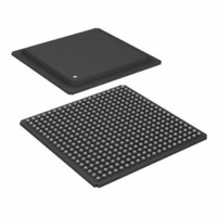
ADSP-21160NCB-100 Analog Devices Inc, ADSP-21160NCB-100 Datasheet - Page 30

ADSP-21160NCB-100
Manufacturer Part Number
ADSP-21160NCB-100
Description
IC,DSP,32-BIT,CMOS,BGA,400PIN,PLASTIC
Manufacturer
Analog Devices Inc
Series
SHARC®r
Type
Floating Pointr
Specifications of ADSP-21160NCB-100
Rohs Status
RoHS non-compliant
Interface
Host Interface, Link Port, Serial Port
Clock Rate
100MHz
Non-volatile Memory
External
On-chip Ram
512kB
Voltage - I/o
3.30V
Voltage - Core
1.90V
Operating Temperature
-40°C ~ 100°C
Mounting Type
Surface Mount
Package / Case
400-BGA
Package
400BGA
Numeric And Arithmetic Format
Floating-Point
Maximum Speed
100 MHz
Ram Size
512 KB
Device Million Instructions Per Second
100 MIPS
Lead Free Status / RoHS Status
Available stocks
Company
Part Number
Manufacturer
Quantity
Price
Company:
Part Number:
ADSP-21160NCB-100
Manufacturer:
Analog Devices Inc
Quantity:
10 000
ADSP-21160N
Three-State Timing—Bus Master, Bus Slave
See
memory interface is disabled (stops driving) or enabled (resumes
driving) relative to CLKIN and the SBTS pin. This timing is
applicable to bus master transition cycles (BTC) and host tran-
sition cycles (HTC) as well as the SBTS pin.
Table 17. Three-State Timing—Bus Master, Bus Slave
1
2
3
4
Parameter
Timing Requirements
t
t
Switching Characteristics
t
t
t
t
t
t
t
t
t
t
t
t
t
t
t
t
t
Strobes = RDx, WRx, DMAGx.
If access aborted by SBTS, then strobes disable before CLKIN [0.25t
In addition to bus master transition cycles, these specs also apply to bus master and bus slave synchronous read/write.
Memory Interface = Address, RDx, WRx, MSx, PAGE, DMAGx, and BMS (in EPROM boot mode).
STSCK
HTSCK
MIENA
MIENS
MIENHG
MITRA
MITRS
MITRHG
DATEN
DATTR
ACKEN
ACKTR
CDCEN
CDCTR
ATRHBG
STRHBG
PTRHBG
BTRHBG
MENHBG
Table 17
and
SBTS Setup Before CLKIN
SBTS Hold After CLKIN
Address/Select Enable After CLKIN
Strobes Enable After CLKIN
HBG Enable After CLKIN
Address/Select Disable After CLKIN
Strobes Disable After CLKIN
HBG Disable After CLKIN
Data Enable After CLKIN
Data Disable After CLKIN
ACK Enable After CLKIN
ACK Disable After CLKIN
CLKOUT Enable After CLKIN
CLKOUT Disable After CLKIN
Address, MSx Disable Before HBG Low
RDx, WRx, DMAGx Disable Before HBG Low
Page Disable Before HBG Low
BMS Disable Before HBG Low
Memory Interface Enable After HBG High
Figure
20. These specifications show how the
3
3
3
3
1
1, 2
CCLK
4
–30–
+ 1.5 (min.), 0.25t
Min
6
2
1.5
1.5
1.5
0.5
0.25t
0.5
0.25t
0.5
1.5
1.5
0.5
t
1.5t
t
t
0.5t
t
CCLK
CK
CK
CK
– 5
+ 0.25t
– 6
CK
CK
CCLK
CCLK
– 3
– 6
– 6.5
– 4
+1
CCLK
CCLK
+ 5 (max.)]
– 6
Max
9
9
9
9
0.25t
8
0.25t
5
9
5
9
t
1.5t
t
t
0.5t
t
CCLK
CK
CK
CK
+6
+ 0.25t
+ 5
CK
CK
+1
CCLK
CCLK
+ 5
+ 1.5
+1.5
+ 7
CCLK
+ 5
Unit
ns
ns
ns
ns
ns
ns
ns
ns
ns
ns
ns
ns
ns
ns
ns
ns
ns
ns
ns
REV. 0


