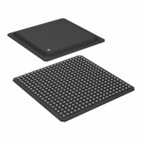
ADSP-21160NCB-100 Analog Devices Inc, ADSP-21160NCB-100 Datasheet - Page 28

ADSP-21160NCB-100
Manufacturer Part Number
ADSP-21160NCB-100
Description
IC,DSP,32-BIT,CMOS,BGA,400PIN,PLASTIC
Manufacturer
Analog Devices Inc
Series
SHARC®r
Type
Floating Pointr
Specifications of ADSP-21160NCB-100
Rohs Status
RoHS non-compliant
Interface
Host Interface, Link Port, Serial Port
Clock Rate
100MHz
Non-volatile Memory
External
On-chip Ram
512kB
Voltage - I/o
3.30V
Voltage - Core
1.90V
Operating Temperature
-40°C ~ 100°C
Mounting Type
Surface Mount
Package / Case
400-BGA
Package
400BGA
Numeric And Arithmetic Format
Floating-Point
Maximum Speed
100 MHz
Ram Size
512 KB
Device Million Instructions Per Second
100 MIPS
Lead Free Status / RoHS Status
Available stocks
Company
Part Number
Manufacturer
Quantity
Price
Company:
Part Number:
ADSP-21160NCB-100
Manufacturer:
Analog Devices Inc
Quantity:
10 000
ADSP-21160N
Asynchronous Read/Write—Host to ADSP-21160N
Use these specifications
Figure
ADSP-21160N, after the host has asserted CS and HBR (low).
Table 15. Read Cycle
Table 16. Write Cycle
Parameter
Timing Requirements
t
t
t
t
t
Switching Characteristics
t
t
t
t
Parameter
Timing Requirements
t
t
t
t
t
t
t
t
t
Switching Characteristics
t
t
SADRDL
HADRDH
WRWH
DRDHRDY
DRDHRDY
SDATRDY
DRDYRDL
RDYPRD
HDARWH
SCSWRL
HCSWRH
SADWRH
HADWRH
WWRL
WRWH
DWRHRDY
SDATWH
HDATWH
DRDYWRL
RDYPWR
19) for asynchronous host processor accesses of an
Address Setup/CS Low Before RDx Low
Address Hold/CS Hold Low After RDx
RDx/WRx High Width
RDx High Delay After REDY (O/D) Disable
RDx High Delay After REDY (A/D) Disable
Data Valid Before REDY Disable from Low
REDY (O/D) or (A/D) Low Delay After RDx Low
REDY (O/D) or (A/D) Low Pulsewidth for Read
Data Disable After RDx High
CS Low Setup Before WRx Low
CS Low Hold After WRx High
Address Setup Before WRx High
Address Hold After WRx High
WRx Low Width
RDx/WRx High Width
WRx High Delay After REDY (O/D) or (A/D) Disable
Data Setup Before WRx High
Data Hold After WRx High
REDY (O/D) or (A/D) Low Delay After WRx/CS Low
REDY (O/D) or (A/D) Low Pulsewidth for Write
(Table
15,
Table
16,
Figure
18, and
–28–
After HBG is returned by the ADSP-21160N, the host can drive
the RDx and WRx pins to access the ADSP-21160N’s internal
memory or IOP registers. HBR and HBG are assumed low for
this timing.
Min
0
2
5
0
0
2
t
1.5
Min
0
0
6
2
t
5
0
5
4
5.75 + 0.5t
CCLK
CK
– 4
+1
CCLK
Max
11
6
Max
11
ns
ns
ns
ns
ns
ns
ns
REV. 0
Unit
ns
ns
Unit
ns
ns
ns
ns
ns
ns
ns
ns
ns
ns
ns


