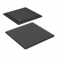
ADSP-21160NCB-100 Analog Devices Inc, ADSP-21160NCB-100 Datasheet - Page 42

ADSP-21160NCB-100
Manufacturer Part Number
ADSP-21160NCB-100
Description
IC,DSP,32-BIT,CMOS,BGA,400PIN,PLASTIC
Manufacturer
Analog Devices Inc
Series
SHARC®r
Type
Floating Pointr
Specifications of ADSP-21160NCB-100
Rohs Status
RoHS non-compliant
Interface
Host Interface, Link Port, Serial Port
Clock Rate
100MHz
Non-volatile Memory
External
On-chip Ram
512kB
Voltage - I/o
3.30V
Voltage - Core
1.90V
Operating Temperature
-40°C ~ 100°C
Mounting Type
Surface Mount
Package / Case
400-BGA
Package
400BGA
Numeric And Arithmetic Format
Floating-Point
Maximum Speed
100 MHz
Ram Size
512 KB
Device Million Instructions Per Second
100 MIPS
Lead Free Status / RoHS Status
Available stocks
Company
Part Number
Manufacturer
Quantity
Price
Company:
Part Number:
ADSP-21160NCB-100
Manufacturer:
Analog Devices Inc
Quantity:
10 000
ADSP-21160N
Capacitive Loading
Output delays and holds are based on standard capacitive loads:
30 pF on all pins (see
how output rise time varies with capacitance.
cally shows how output delays and holds vary with load
capacitance. (Note that this graph or derating does not apply to
output disable delays; see Output Disable Time
The graphs of
linear outside the ranges shown.
12
Figure 31. Typical Output Rise Time (20%–80%,
V
Figure 32. Typical Output Rise Time (20%–80%,
V
20
18
16
14
10
8
6
4
2
25
20
15
10
0
DDEXT
DDEXT
5
0
0
0
= Max) vs. Load Capacitance
= Min) vs. Load Capacitance
Figure
Y = 0.0716x
50
50
Figure
31,
Y = 0.0813x
LOAD CAPACITANCE – pF
LOAD CAPACITANCE – pF
+ 2.9043
Figure
100
100
29).
Y = 0.0751x
RISE TIME
Y = 0.0834x
TBD
+ 2.312
RISE TIME
TBD
32, and
Figure 31
FALL TIME
150
FALL TIME
150
+ 1.4882
+ 1.0653
Figure 33
and
200
Figure 33
200
Figure 32
on Page
may not be
250
250
graphi-
41.)
show
–42–
Environmental Conditions
The ADSP-21160NKB-100 and ADSP-21160NCB-100 are
provided in a 400-Ball Metric PBGA (Plastic Ball Grid Array)
package.
Thermal Characteristics
The ADSP-21160N is specified for a case temperature (T
To ensure that the T
a heatsink and/or an air flow source may be used. Use the cen-
terblock of ground pins (PBGA balls: F7-14, G7-14, H7-14,
J7-14, K7-14, L7-14, M-14, N7-14, P7-14, R7-15) to provide
thermal pathways to the printed circuit board’s ground plane. A
heatsink should be attached to the ground plane (as close as
possible to the thermal pathways) with a thermal adhesive.
Table 31. Airflow Over Package Versus
1
Airflow (Linear Ft./Min.)
CA
JC
T
of package)
PD = Power dissipation in W (this value depends upon
the specific application; a method for calculating PD is
shown under Power Dissipation).
CA
JB
CASE
= 3.6 °C/W.
(°C/W)
Figure 33. Typical Output Delay or Hold vs. Load
Capacitance (at Max Case Temperature)
= 6.46°C/W
= Value from
12
10
–4
–2
4
= Case temperature (measured on top surface
8
6
2
0
0
Y = 0.0716x
1
T
CASE
50
CASE
– 3.9037
Table
=
LOAD CAPACITANCE – pF
data sheet specification is not exceeded,
T
AMB
100
31.
+
0
12.13
PD
150
CA
200
9.86
CA
200
400
8.7
250
REV. 0
CASE
).


