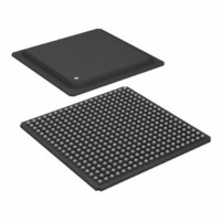
ADSP-21160NCB-100 Analog Devices Inc, ADSP-21160NCB-100 Datasheet - Page 4

ADSP-21160NCB-100
Manufacturer Part Number
ADSP-21160NCB-100
Description
IC,DSP,32-BIT,CMOS,BGA,400PIN,PLASTIC
Manufacturer
Analog Devices Inc
Series
SHARC®r
Type
Floating Pointr
Specifications of ADSP-21160NCB-100
Rohs Status
RoHS non-compliant
Interface
Host Interface, Link Port, Serial Port
Clock Rate
100MHz
Non-volatile Memory
External
On-chip Ram
512kB
Voltage - I/o
3.30V
Voltage - Core
1.90V
Operating Temperature
-40°C ~ 100°C
Mounting Type
Surface Mount
Package / Case
400-BGA
Package
400BGA
Numeric And Arithmetic Format
Floating-Point
Maximum Speed
100 MHz
Ram Size
512 KB
Device Million Instructions Per Second
100 MIPS
Lead Free Status / RoHS Status
Available stocks
Company
Part Number
Manufacturer
Quantity
Price
Company:
Part Number:
ADSP-21160NCB-100
Manufacturer:
Analog Devices Inc
Quantity:
10 000
ADSP-21160N
GENERAL DESCRIPTION
The ADSP-21160N SHARC DSP is the second iteration of the
ADSP-21160. Built in a 0.18 micron CMOS process, it offers
higher performance and lower power consumption than its pre-
decessor, the ADSP-21160M. Easing portability, the ADSP-
21160N is application source code compatible with first genera-
tion ADSP-2106x SHARC DSPs in SISD (Single Instruction,
Single Data) mode. To take advantage of the processor’s SIMD
(Single Instruction, Multiple Data) capability, some code
changes are needed. Like other SHARCs, the ADSP-21160N is
a 32-bit processor that is optimized for high performance DSP
applications. The ADSP-21160N includes a 100 MHz core, a
dual-ported on-chip SRAM, an integrated I/O processor with
multiprocessing support, and multiple internal buses to eliminate
I/O bottlenecks.
The ADSP-21160N introduces Single-Instruction,
Multiple-Data (SIMD) processing. Using two computational
units (ADSP-2106x SHARC DSPs have one), the ADSP-
21160N can double performance versus the ADSP-2106x on a
range of DSP algorithms.
Fabricated in a state of the art, high speed, low power CMOS
process, the ADSP-21160N has a 10 ns instruction cycle time.
With its SIMD computational hardware running at 100 MHz,
the ADSP-21160N can perform 600 million math operations per
second.
Table 1
Table 1. ADSP-21160N Benchmarks
1
These benchmarks provide single-channel extrapolations of
measured dual-channel processing performance. For more infor-
mation on benchmarking and optimizing DSP code for single-
and dual-channel processing, see the Analog Devices website
(www.analog.com).
The ADSP-21160N continues SHARC’s industry-leading
standards of integration for DSPs, combining a high performance
32-bit DSP core with integrated, on-chip system features. These
features include a 4M-bit dual ported SRAM memory, host
processor interface, I/O processor that supports 14 DMA
channels, two serial ports, six link ports, external parallel bus,
and glueless multiprocessing.
Benchmark Algorithm
1024 Point Complex FFT (Radix 4, with
reversal)
FIR Filter (per tap)
IIR Filter (per biquad)
Matrix Multiply (pipelined)
[3 3]
[4 4]
Divide (y/x)
Inverse Square Root
DMA Transfer Rate
Specified in SISD mode. Using SIMD, the same benchmark applies for
two sets of computations.For example, two sets of biquad operations can
be performed in the same amount of time as the SISD mode benchmark.
shows performance benchmarks for the ADSP-21160N.
[3 1]
[4 1]
Speed
171 µs
5 ns
40 ns
30 ns
37 ns
60 ns
90 ns
800M byte/s
1
1
1
–4–
The functional block diagram
of the ADSP-21160N, illustrating the following architectural
features:
Figure 1
ing system appears in
ADSP-21160N Family Core Architecture
The ADSP-21160N includes the following architectural features
of the ADSP-2116x family core. The ADSP-21160N is code
compatible at the assembly level with the ADSP-2106x and
ADSP-21161.
(OPTIONAL)
(OPTIONAL)
(OPTIONAL)
DEVICES
Two processing elements, each made up of an ALU, Mul-
tiplier, Shifter, and Data Register File
Data Address Generators (DAG1, DAG2)
Program sequencer with instruction cache
PM and DM buses capable of supporting four 32-bit data
transfers between memory and the core every core
processor cycle
Interval timer
On-Chip SRAM (4M bits)
External port that supports:
DMA controller
Serial ports and link ports
JTAG test access port
(6 MAX)
SERIAL
DEVICE
DEVICE
SERIAL
CLOCK
LINK
Interfacing to off-chip memory peripherals
Glueless multiprocessing support for six ADSP-
21160N SHARCs
Host port
shows a typical single-processor system. A multiprocess-
4
3
4
Figure 1. Single-Processor System
CLKIN
EBOOT
LBOOT
IRQ2–0
FLAG3–0
TIMEXP
LXCLK
LXACK
LXDAT7–0
TCLK0
RCLK0
TFS0
RSF0
DT0
DR0
TCLK1
RCLK1
TFS1
RSF1
DT1
DR1
RPBA
ID2–0
CLK_CFG3–0
ADSP-21160
RESET
Figure
ADDR31–0
DATA63–0
DMAG1–2
DMAR1–2
CLKOUT
JTAG
MS3–0
BR1–6
PAGE
REDY
BRST
SBTS
BMS
WRx
ACK
HBR
HBG
RDx
4.
6
CIF
CS
PA
on Page 1
shows a block diagram
DATA
ADDR
DATA
CS
ADDR
DATA
OE
WE
ACK
ADDR
DATA
CS
PROCESSOR
(OPTIONAL)
INTERFACE
DMA DEVICE
(OPTIONAL)
(OPTIONAL)
(OPTIONAL)
MEMORY/
HOST
REV. 0
DEVICES
MAPPED
EPROM
BOOT


