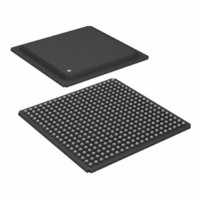
ADSP-21160NCB-100 Analog Devices Inc, ADSP-21160NCB-100 Datasheet - Page 14

ADSP-21160NCB-100
Manufacturer Part Number
ADSP-21160NCB-100
Description
IC,DSP,32-BIT,CMOS,BGA,400PIN,PLASTIC
Manufacturer
Analog Devices Inc
Series
SHARC®r
Type
Floating Pointr
Specifications of ADSP-21160NCB-100
Rohs Status
RoHS non-compliant
Interface
Host Interface, Link Port, Serial Port
Clock Rate
100MHz
Non-volatile Memory
External
On-chip Ram
512kB
Voltage - I/o
3.30V
Voltage - Core
1.90V
Operating Temperature
-40°C ~ 100°C
Mounting Type
Surface Mount
Package / Case
400-BGA
Package
400BGA
Numeric And Arithmetic Format
Floating-Point
Maximum Speed
100 MHz
Ram Size
512 KB
Device Million Instructions Per Second
100 MIPS
Lead Free Status / RoHS Status
Available stocks
Company
Part Number
Manufacturer
Quantity
Price
Company:
Part Number:
ADSP-21160NCB-100
Manufacturer:
Analog Devices Inc
Quantity:
10 000
ADSP-21160N
SPECIFICATIONS
RECOMMENDED OPERATING CONDITIONS
1
2
3
ELECTRICAL CHARACTERISTICS
1
2
3
4
5
Parameter
V
AV
V
T
V
V
V
Specifications subject to change without notice.
Parameter
V
V
I
I
I
I
I
I
I
I
I
I
I
I
I
I
I
I
I
I
I
I
I
AI
C
Specifications subject to change without notice.
See Environmental Conditions
Applies to input and bidirectional pins: DATA63–0, ADDR31–0, RDx, WRx, ACK, SBTS, IRQ2–0, FLAG3–0, HBG, CS, DMAR1, DMAR2, BR6–1,
Applies to input pins: CLKIN, RESET, TRST.
Applies to output and bidirectional pins: DATA63–0, ADDR31–0, MS3–0, RDx, WRx, PAGE, CLKOUT, ACK, FLAG3–0, TIMEXP, HBG, REDY,
See Output Drive Currents
Applies to input pins: SBTS, IRQ2–0, HBR, CS, ID2–0, RPBA, EBOOT, LBOOT, CLKIN, RESET, TCK, CLK_CFG3-0.
Applies to input pins with internal pull-ups: DR0, DR1.
Applies to input pins with internal pull-ups: DMARx, TMS, TDI, TRST.
ID2–0, RPBA, PA, BRST, TFS0, TFS1, RFS0, RFS1, LxDAT3–0, LxCLK, LxACK, EBOOT, LBOOT, BMS, TMS, TDI, TCK, HBR, DR0, DR1,
TCLK0, TCLK1, RCLK0, RCLK1.
DMAG1, DMAG2, BR6–1, PA, BRST, CIF, DT0, DT1, TCLK0, TCLK1, RCLK0, RCLK1, TFS0, TFS1, RFS0, RFS1, LxDAT3–0, LxCLK, LxACK,
BMS, TDO, EMU.
IH
IL
IHC
ILC
IKH
IKL
IKH-OD
IKL-OD
ILPU1
ILPU2
OZH
OZL
OZHPD
OZLPU1
OZLPU2
OZHA
OZLA
DD-INPEAK
DD-INHIGH
DD-INLOW
DD-IDLE
DDINT
DDEXT
IH1
IH2
IL
OH
OL
CASE
IN
DD
DD
High Level Output Voltage
Low Level Output Voltage
High Level Input Current
Low Level Input Current
CLKIN High Level Input Current
CLKIN Low Level Input Current
Keeper High Load Current
Keeper Low Load Current
Keeper High Overdrive Current
Keeper Low Overdrive Current
Low Level Input Current Pull-Up1
Low Level Input Current Pull-Up2
Three-State Leakage Current
Three-State Leakage Current
Three-State Leakage Current Pull-Down
Three-State Leakage Current Pull-Up1
Three-State Leakage Current Pull-Up2
Three-State Leakage Current
Three-State Leakage Current
Supply Current (Internal)
Supply Current (Internal)
Supply Current (Internal)
Supply Current (Idle)
Supply Current (Analog)
Input Capacitance
Internal (Core) Supply Voltage
Analog (PLL) Supply Voltage
External (I/O) Supply Voltage
Case Operating Temperature
High Level Input Voltage,
High Level Input Voltage,
Low Level Input Voltage,
on Page 40
on Page 42
19, 20
for typical drive current capabilities.
18
for information on thermal specifications.
6
3
3, 4, 5
15
16
17
1
7
1
7
10, 11, 12, 13
10
14
14
2, 3
7, 8, 9
2
3
7, 8, 9
@ V
@ V
6
@ V
6
1
4
5
DDEXT
DDEXT
DDEXT
11
12
13
=Max
=Max
=Min
Test Conditions
@ V
@ V
@ V
@ V
@ V
@ V
@ V
@ V
@ V
@ V
@ V
@ V
@ V
@ V
@ V
@ V
@ V
@ V
@ V
t
t
t
t
@AV
f
CCLK
CCLK
CCLK
CCLK
IN
–14–
=1 MHz, T
DDEXT
DDEXT
DDEXT
DDEXT
DDEXT
DDEXT
DDEXT
DDEXT
DDEXT
DDEXT
DDEXT
DDEXT
DDEXT
DDEXT
DDEXT
DDEXT
DDEXT
DDEXT
DDEXT
=10.0 ns, V
=10.0 ns, V
=10.0 ns, V
=10.0 ns, V
DD
=Max
=Max, V
C Grade
Min
1.8
1.8
3.13
– 40
2.0
2.0
–0.5
=Min, I
= Max, V
= Max, V
= Max, V
= Max, V
= Max
= Max
=Min, I
=Max, V
=Max, V
=Max, V
=Max, V
=Max, V
=Max, V
=Max, V
=Max, V
=Max, V
=Max, V
CASE
DDINT
DDINT
DDINT
DDINT
=25°C, V
Max
2.0
2.0
3.47
+100
V
V
+0.8
OH
OL
IN
IN
IN
IN
IN
IN
IN
IN
IN
IN
IN
IN
IN
IN
IN
DDEXT
DDEXT
=4.0 mA
=–2.0 mA
=V
=V
=0 V
=0 V
=0 V
=0 V
=V
=0 V
=0 V
=V
=0 V
= V
= 0 V
= 2.0 V
= 0.8 V
=Max
=Max
=Max
=Max
DD
DD
DD
DD
+0.5
+0.5
DDEXT
Max
Max
Max
Max
IN
2
=2.5 V
2
Max
K Grade
Min
1.8
1.8
3.13
0
2.0
2.0
–0.5
Min
2.4
–250
–300
300
50
Max
2.0
2.0
3.47
85
V
V
+0.8
DDEXT
DDEXT
Max
0.4
10
10
25
25
–50
200
250
500
10
10
250
250
500
25
4
960
715
550
450
10
4.7
+0.5
+0.5
Unit
V
V
µA
µA
µA
µA
µA
µA
µA
µA
µA
µA
µA
µA
µA
µA
µA
µA
mA
mA
mA
mA
mA
mA
pF
REV. 0
Unit
V
V
V
ºC
V
V
V


