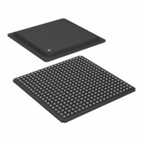
ADSP-21160NCB-100 Analog Devices Inc, ADSP-21160NCB-100 Datasheet - Page 34

ADSP-21160NCB-100
Manufacturer Part Number
ADSP-21160NCB-100
Description
IC,DSP,32-BIT,CMOS,BGA,400PIN,PLASTIC
Manufacturer
Analog Devices Inc
Series
SHARC®r
Type
Floating Pointr
Specifications of ADSP-21160NCB-100
Rohs Status
RoHS non-compliant
Interface
Host Interface, Link Port, Serial Port
Clock Rate
100MHz
Non-volatile Memory
External
On-chip Ram
512kB
Voltage - I/o
3.30V
Voltage - Core
1.90V
Operating Temperature
-40°C ~ 100°C
Mounting Type
Surface Mount
Package / Case
400-BGA
Package
400BGA
Numeric And Arithmetic Format
Floating-Point
Maximum Speed
100 MHz
Ram Size
512 KB
Device Million Instructions Per Second
100 MIPS
Lead Free Status / RoHS Status
Available stocks
Company
Part Number
Manufacturer
Quantity
Price
Company:
Part Number:
ADSP-21160NCB-100
Manufacturer:
Analog Devices Inc
Quantity:
10 000
ADSP-21160N
Link Ports —Receive, Transmit
For Link Ports, see
Figure
relative to link clock, is required to determine the maximum
allowable skew that can be introduced in the transmission path,
between LDATA and LCLK. Setup skew is the maximum delay
that can be introduced in LDATA, relative to LCLK (setup
skew = t
Table 19. Link Ports—Receive
1
Table 20. Link Ports—Transmit
Parameter
Timing Requirements
t
t
t
t
t
Switching Characteristics
t
Parameter
Timing Requirements
t
t
Switching Characteristics
t
t
t
t
t
LACK goes low with t
SLDCL
HLDCL
LCLKIW
LCLKRWL
LCLKRWH
DLALC
SLACH
HLACH
DLDCH
HLDCH
LCLKTWL
LCLKTWH
DLACLK
23. Calculation of link receiver data setup and hold,
LCLKTWH
RECEIVE
LCLK
LDAT(7:0)
LACK (OUT)
minimum – t
Table
Data Setup Before LCLK Low
Data Hold After LCLK Low
LCLK Period
LCLK Width Low
LCLK Width High
LACK Low Delay After LCLK High
LACK Setup Before LCLK High
LACK Hold After LCLK High
Data Delay After LCLK High
Data Hold After LCLK High
LCLK Width Low
LCLK Width High
LCLK Low Delay After LACK High
DLALC
19,
relative to rise of LCLK after first nibble, but does not go low if the receiver’s link buffer is not about to fill.
DLDCH
Table
– t
20,
SLDCL
Figure
). Hold skew is the
t
LCLKRWH
22, and
Figure 22. Link Ports—Receive
t
SLDCL
IN
1
t
–34–
LCLKIW
Min
14
–2
–2
0.5t
0.5t
0.5t
maximum delay that can be introduced in LCLK, relative to
LDATA (hold skew = t
culations made directly from speed specifications result in
unrealistically small skew times, because they include multiple
tester guardbands.
Note that there is a two-cycle effect latency between the link port
enable instruction and the DSP enabling the link port.
t
HLDCL
LCLK
LCLK
LCLK
+4
– .5
– .5
t
LCLKRWL
Min
2.5
3
t
4
4
9
LCLK
LCLKTWL
t
DLALC
Max
4
0.5t
0.5t
3/2t
minimum + t
LCLK
LCLK
LCLK
+.5
+.5
Max
17
+11
HLDCH
– t
HLDCL
ns
ns
ns
ns
ns
ns
ns
ns
ns
ns
REV. 0
Unit
ns
Unit
ns
ns
). Cal-


