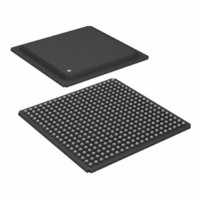
ADSP-21160NCB-100 Analog Devices Inc, ADSP-21160NCB-100 Datasheet - Page 23

ADSP-21160NCB-100
Manufacturer Part Number
ADSP-21160NCB-100
Description
IC,DSP,32-BIT,CMOS,BGA,400PIN,PLASTIC
Manufacturer
Analog Devices Inc
Series
SHARC®r
Type
Floating Pointr
Specifications of ADSP-21160NCB-100
Rohs Status
RoHS non-compliant
Interface
Host Interface, Link Port, Serial Port
Clock Rate
100MHz
Non-volatile Memory
External
On-chip Ram
512kB
Voltage - I/o
3.30V
Voltage - Core
1.90V
Operating Temperature
-40°C ~ 100°C
Mounting Type
Surface Mount
Package / Case
400-BGA
Package
400BGA
Numeric And Arithmetic Format
Floating-Point
Maximum Speed
100 MHz
Ram Size
512 KB
Device Million Instructions Per Second
100 MIPS
Lead Free Status / RoHS Status
Available stocks
Company
Part Number
Manufacturer
Quantity
Price
Company:
Part Number:
ADSP-21160NCB-100
Manufacturer:
Analog Devices Inc
Quantity:
10 000
Synchronous Read/Write—Bus Master
See
facing to external memory systems that require CLKIN—relative
timing or for accessing a slave ADSP-21160N (in multiprocessor
memory space). These synchronous switching characteristics are
also valid during asynchronous memory reads and writes except
where noted (see Memory Read–Bus Master
Table 12. Synchronous Read/Write—Bus Master
1
2
REV. 0
Parameter
Timing Requirements
t
t
t
t
Switching Characteristics
t
t
t
t
t
t
t
t
t
t
t
t
t
t
Applies to broadcast write, master precharge of ACK.
Applies only when the DSP drives a bus operation; CLKOUT held inactive or three-state otherwise. For more information, see the System Design chapter
SSDATI
HSDATI
SACKC
HACKC
DADDO
HADDO
DPGO
DRDO
DWRO
DRWL
DDATO
HDATO
DACKMO
ACKMTR
DCKOO
CKOP
CKWH
CKWL
in the ADSP-2116x SHARC DSP Hardware Reference.
Table 12
and
Figure
Data Setup Before CLKIN
Data Hold After CLKIN
ACK Setup Before CLKIN
ACK Hold After CLKIN
Address, MSx, BMS, BRST, CIF Delay After CLKIN
Address, MSx, BMS, BRST, CIF Hold After CLKIN
PAGE Delay After CLKIN
RDx High Delay After CLKIN
WRx High Delay After CLKIN
RDx/WRx Low Delay After CLKIN
Data Delay After CLKIN
Data Hold After CLKIN
ACK Delay After CLKIN
ACK Disable Before CLKIN
CLKOUT Delay After CLKIN
CLKOUT Period
CLKOUT Width High
CLKOUT Width Low
15. Use these specifications for inter-
on Page 21
1
1
and
–23–
Memory Write–Bus Master
ADSP-21160N, these switching characteristics must meet the
slave’s timing requirements for synchronous read/writes (see Syn-
chronous Read/Write–Bus Slave
21160N must also meet these (bus master) timing requirements
for data and acknowledge setup and hold times.
Min
5.5
1
0.5t
1
1.5
1.5
0.25t
0.25t
0.25t
1.5
0.5
t
t
t
3
–3
CK
CK
CK
/2 – 2
/2 – 2
– 1
CCLK
CCLK
CCLK
CCLK
+3
on Page
– 1
– 1
– 1
on Page
ADSP-21160N
22). When accessing a slave
Max
10
11
0.25t
0.25t
0.25t
0.25t
5
t
t
t
9
CK
CK
CK
2
/2+2
/2+2
25). The slave ADSP-
+1
CCLK
CCLK
CCLK
CCLK
2
2
+9
+9
+9
+9
Unit
ns
ns
ns
ns
ns
ns
ns
ns
ns
ns
ns
ns
ns
ns
ns
ns
ns
ns


