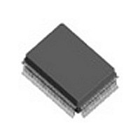
IDT82V2108PXG IDT, Integrated Device Technology Inc, IDT82V2108PXG Datasheet - Page 279

IDT82V2108PXG
Manufacturer Part Number
IDT82V2108PXG
Description
IC FRAMER T1/J1/E1 8CH 128-PQFP
Manufacturer
IDT, Integrated Device Technology Inc
Datasheet
1.IDT82V2108PX8.pdf
(292 pages)
Specifications of IDT82V2108PXG
Controller Type
T1/E1/J1 Framer
Interface
Parallel
Voltage - Supply
2.97 V ~ 3.63 V
Current - Supply
160mA
Operating Temperature
-40°C ~ 85°C
Mounting Type
Surface Mount
Package / Case
128-MQFP, 128-PQFP
Screening Level
Industrial
Mounting
Surface Mount
Operating Temperature (min)
-40C
Operating Temperature (max)
85C
Lead Free Status / RoHS Status
Lead free / RoHS Compliant
Other names
82V2108PXG
Available stocks
Company
Part Number
Manufacturer
Quantity
Price
Company:
Part Number:
IDT82V2108PXG
Manufacturer:
IDT, Integrated Device Technology Inc
Quantity:
10 000
Part Number:
IDT82V2108PXG
Manufacturer:
IDT
Quantity:
20 000
Company:
Part Number:
IDT82V2108PXG8
Manufacturer:
IDT, Integrated Device Technology Inc
Quantity:
10 000
- Current page: 279 of 292
- Download datasheet (3Mb)
IDT82V2108
6.1
ISTER (IR)
to select the test to be executed or the data register to be accessed or
both.
IEEE STD 1149.1 JTAG Test Access Port
Table 66: IR Code
IR CODE INSTRUCTION
0 0 0
0 1 0
0 0 1
1 1 1
1 0 0
1 0 1
0 1 1
The IR (Instruction Register) with instruction decode block is used
JTAG INSTRUCTIONS AND INSTRUCTION REG-
PRELOAD
SAMPLE /
BYPASS
EXTEST
IDCODE
CLAMP
HIGHZ
The external test instruction allows testing of the interconnection to other devices. When the current instruction is the EXTEST instruc-
tion, the boundary scan register is placed between TDI and TDO. The signal on the input pins can be sampled by loading the boundary
scan register using the Capture-DR state. The sampled values can then be viewed by shifting the boundary scan register using the Shift-
DR state. The signal on the output pins can be controlled by loading patterns shifted in through input TDI into the boundary scan register
using the Update-DR state.
The SAMPLE/PRELOAD instruction is used to allow scanning of the boundary-scan register without causing interference to the normal
operation of the on-chip system logic. Data received at system input pins is supplied without modification to the on-chip system logic;
data from the on-chip system logic is driven without modification through the system output pins. SAMPLE allows a snapshot to be taken
of the data flowing from the system pins to the on-chip system logic or vice versa, without interfering with the normal operation of the
assembled board. PRELOAD allows an initial data pattern to be placed at the latched parallel outputs of boundary-scan register cells
prior to selection of another boundary-scan test operation.
The identification instruction is used to connect the identification register between TDI and TDO. The device’s identification code can then
be shifted out using the Shift-DR state.
The BYPASS instruction shifts data from input TDI to output TDO with one TCK clock period delay. The instruction is used to bypass the
device.
This instruction allows the state of the signals driven from device pins to be determined from the boundary-scan register while the bypass
register is selected as the serial path between TDI and TDO. The signals driven from the device pins will not change while the CLAMP
instruction is selected.
Use of the HIGHZ instruction places the device in a state in which all of its system logic outputs are placed in an inactive drive state (e.g.,
high impedance). In this state, and in-circuit test system may drive signals onto the connections normally driven by a device output with-
out incurring the risk of damage to the device.
(for manufactory test)
269
Table 66 for details of the codes and the instructions related.
COMMENTS
The instructions are shifted in LSB first to this 3-bit register. See
T1 / E1 / J1 OCTAL FRAMER
March 5, 2009
Related parts for IDT82V2108PXG
Image
Part Number
Description
Manufacturer
Datasheet
Request
R

Part Number:
Description:
TRANSLATION DEVICE DPI 80-PQFP
Manufacturer:
IDT, Integrated Device Technology Inc
Datasheet:

Part Number:
Description:
IDT PART
Manufacturer:
IDT, Integrated Device Technology Inc
Datasheet:

Part Number:
Description:
IC LIU T1/E1/J1 OCTAL 256PBGA
Manufacturer:
IDT, Integrated Device Technology Inc
Datasheet:

Part Number:
Description:
IC FREQ TIMING GENERATOR 28TSSOP
Manufacturer:
IDT, Integrated Device Technology Inc
Datasheet:

Part Number:
Description:
IC CLK DVR PLL 1:10 40VFQFPN
Manufacturer:
IDT, Integrated Device Technology Inc
Datasheet:

Part Number:
Description:
IC CLK FANOUT BUFFER 1:18 32LQFP
Manufacturer:
IDT, Integrated Device Technology Inc
Datasheet:

Part Number:
Description:
IC CLK FANOUT BUFFER 1:18 32LQFP
Manufacturer:
IDT, Integrated Device Technology Inc
Datasheet:

Part Number:
Description:
IC CK505 VREG/RES 56TSSOP
Manufacturer:
IDT, Integrated Device Technology Inc
Datasheet:

Part Number:
Description:
IC SDRAM CLK DVR 1:10 48-TSSOP
Manufacturer:
IDT, Integrated Device Technology Inc
Datasheet:

Part Number:
Description:
IC CLK DVR PLL 1:10 48TSSOP
Manufacturer:
IDT, Integrated Device Technology Inc
Datasheet:

Part Number:
Description:
IC FLEXPC CLK PROGR P4 56-TSSOP
Manufacturer:
IDT, Integrated Device Technology Inc
Datasheet:

Part Number:
Description:
IC FLEXPC CLK PROGR P4 56-TSSOP
Manufacturer:
IDT, Integrated Device Technology Inc
Datasheet:

Part Number:
Description:
IC FLEXPC CLK PROGR P4 56-SSOP
Manufacturer:
IDT, Integrated Device Technology Inc
Datasheet:

Part Number:
Description:
IC PLL CLK DRIVER 2.5V 28-TSSOP
Manufacturer:
IDT, Integrated Device Technology Inc
Datasheet:

Part Number:
Description:
IC CLOCK DRIVER 2.5V 24-TSSOP
Manufacturer:
IDT, Integrated Device Technology Inc
Datasheet:


