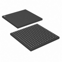
DS26324GNA3+ Maxim Integrated Products, DS26324GNA3+ Datasheet - Page 12

DS26324GNA3+
Manufacturer Part Number
DS26324GNA3+
Description
IC LIU E1/T1/J1 3.3V 256-CSBGA
Manufacturer
Maxim Integrated Products
Type
Line Interface Units (LIUs)r
Datasheet
1.DS26324GNTR.pdf
(120 pages)
Specifications of DS26324GNA3+
Number Of Drivers/receivers
16/16
Protocol
LIN
Voltage - Supply
3.135 V ~ 3.465 V
Mounting Type
Surface Mount
Package / Case
256-CSBGA
Lead Free Status / RoHS Status
Lead free / RoHS Compliant
RPOS10/RDATA10
RPOS11/RDATA11
RPOS12/RDATA12
RPOS13/RDATA13
RPOS14/RDATA14
RPOS15/RDATA15
RPOS16/RDATA16
RPOS1/RDATA1
RPOS2/RDATA2
RPOS3/RDATA3
RPOS4/RDATA4
RPOS5/RDATA5
RPOS6/RDATA6
RPOS7/RDATA7
RPOS8/RDATA8
RPOS9/RDATA9
RNEG10/CV10
RNEG11/CV11
RNEG12/CV12
RNEG13/CV13
RNEG14/CV14
RNEG15/CV15
RNEG16/CV16
RNEG1/CV1
RNEG2/CV2
RNEG3/CV3
RNEG4/CV4
RNEG5/CV5
RNEG6/CV6
RNEG7/CV7
RNEG8/CV8
RNEG9/CV9
TCLK10
TCLK11
TCLK12
TCLK13
TCLK14
TCLK15
TCLK16
TCLK1
TCLK2
TCLK3
TCLK4
TCLK5
TCLK6
TCLK7
TCLK8
TCLK9
NAME
M12
M14
G12
M10
M13
K11
K12
F14
E12
C11
D12
D11
K13
E14
C12
C10
P11
K10
F13
F11
E10
PIN
L10
L14
M7
M9
M3
G4
G9
H6
N7
C8
G5
C9
C7
F5
L8
P9
F4
F3
L3
L4
K8
P8
E5
E3
K4
L7
J3
tri-state
tri-state
TYPE
O,
O,
I
Transmit Clock for Channels 1–16. The transmit clock has to be
1.544MHz for T1 or 2.048MHz for E1 mode. TCLKn is the clock used
to sample the data TPOS/TNEG or TDAT on the falling edge. The
expected TCLK can be inverted.
If TCLKn is ‘high’ for 16 or more MCLKs, then transmit all ones
(TAOs) is sent to the line side of the corresponding transmit channel.
When TCLKn starts clocking again, normal operation will begin again
for the corresponding transmit channel.
If TCLKn is ‘low’ for 64 or more MCLKs, then the corresponding
transmit channel on the line side will power-down and be put into high
impedance. When TCLKn starts clocking again the corresponding
transmit channel will power-up and come out of high impedance.
Receive Positive Data Output for Channels 1–16. In dual-rail mode
the NRZ data output indicates a positive pulse on RTIP/RRING. Upon
detecting an LOS, AIS can be inserted if the AISEL bit in the
(0Fh) register is set; otherwise, the pins will be active. AIS insertion
can also be controlled on an individual LIU basis by the
register. If a given receiver is in power-down mode, the associated
RPOS pin is high impedance.
Receive Data Output for Channels 1–16. In single-rail mode, NRZ
data is sent out on this pin. If a given receiver is in power-down mode,
the associated RPOS pin is high impedance.
Note: During an LOS condition, the RPOS/RDATA outputs remain
active.
Receive Negative Data Output for Channels 1–16. In dual-rail
mode the NRZ data output indicates a negative pulse on
RTIP/RRING. Upon detecting a LOS, AIS can be inserted if AISEL bit
in the
insertion can also be controlled on an individual LIU basis by
register. If a given receiver is in power-down mode, the associated
RNEG pin is high impedance.
Code Violation for Channels 1–16. In single-rail mode, bipolar
violation, code violation, and excessive zeros are reported on CVn. If
HDB3 or B8ZS is not selected, this pin indicates only BPVs. If a given
receiver is in power-down mode, the associated CV pin is high
impedance.
DS26324 3.3V, 16-Channel, E1/T1/J1 Short-Haul Line Interface Unit
GC
12 of 120
register is set; otherwise, the pins will be active. AIS
FUNCTION
IAISEL
GC
IAISEL
(05h)


