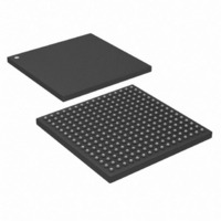
DS26324GNA3+ Maxim Integrated Products, DS26324GNA3+ Datasheet - Page 120

DS26324GNA3+
Manufacturer Part Number
DS26324GNA3+
Description
IC LIU E1/T1/J1 3.3V 256-CSBGA
Manufacturer
Maxim Integrated Products
Type
Line Interface Units (LIUs)r
Datasheet
1.DS26324GNTR.pdf
(120 pages)
Specifications of DS26324GNA3+
Number Of Drivers/receivers
16/16
Protocol
LIN
Voltage - Supply
3.135 V ~ 3.465 V
Mounting Type
Surface Mount
Package / Case
256-CSBGA
Lead Free Status / RoHS Status
Lead free / RoHS Compliant
- Current page: 120 of 120
- Download datasheet (2Mb)
Maxim cannot assume responsibility for use of any circuitry other than circuitry entirely embodied in a Maxim product. No circuit patent licenses are implied. Maxim
reserves the right to change the circuitry and specifications without notice at any time.
M a x i m I n t e g r a t e d P r o d u c t s , 1 2 0 S a n G a b r i e l D r iv e , S u n n y v a le , C A 9 4 0 8 6 4 0 8- 7 3 7 - 7 6 0 0
© 2011 Maxim Integrated Products
REVISION
053107
012108
DATE
3/11
Changed GMC to BGMC; changed bits 7, 6, and 5 from Reserved to BERTDIR,
BMCKS, and BTCKS.
In the GC register (LIUs 1–8), changed bit 7 from Reserved to RIMPMS and bit 2
from RTCTL to CRIMP (see also page 44, Table 6-5).
In the GC register (LIUs 9–16), changed bit 7 from Reserved to RIMPMS and
changed bit 2 from Reserved to CALEN (see also page 44, Table 6-5).
For TST, changed bits 7, 6, and 5 from Reserved to JABWS1, JABWS0, and
RHPMC.
In the bit 7 (RIMPON) description, changed GC.RTCTL to TST.RHPMC; added
note to bit description.
Changed bit description for OE bits 7 to 0.
For EZDE, corrected bit names for LIUs 1–16 from EXZDE[1:16] to EZDE[1:16];
changed bit description to say “Excessive zero detection is only relevant when
HDB3 or B8ZS decoding is enabled.” For CVDEB, changed bit description to say
“Code violation detection is only relevant when HDB3 decoding is enabled (LCS
register).”
Added note to bit 3 (RSMM1:RSSM4) description and updated descriptions for bits
6–4 and 2–0 (deleted “When” from each sentence for clarity).
Updated package drawing information.
In Table 12-1, deleted “Power Dissipation in Package”; added new Table 12-2.
Package Power Dissipation (for Thermal Considerations) and Table 12-3. Per-
Channel Power-Down Saving (for Thermal Considerations).
Table 8-3: added “Note 1: Specifications to -40°C are guaranteed by design (GBD)
and not production tested.”
Table 9-3, 9-4, 9-5, and 9-6: added “Note 1: The timing parameters in this table are
guaranteed by design (GBD).”
Changed the GC (2Fh) register bit 1 (JAPS) description.
Figure 10-1 in Section 10 PIN CONFIGURATION: Corrected cell R9. Changed
from DVSS to RESREF.
Pb-free ordering information added
Table 4-1. PIN DESCRIPTION. TRSTB Function description changed. Replaced
“floating” with “unconnected”
Section 8 DC ELECTRICAL CHARACTERIZATION: Soldering information in
ABSOLUTE MAXIMUM RATINGS table updated
DS26324 3.3V, 16-Channel, E1/T1/J1 Short-Haul Line Interface Unit
DESCRIPTION
120 of 120
Maxim is a registered trademark of Maxim Integrated Products, Inc.
71, 72, 73, 74
99, 102, 105,
CHANGED
PAGES
117
118
108
115
53
56
57
58
60
61
65
97
57
15
97
1
Related parts for DS26324GNA3+
Image
Part Number
Description
Manufacturer
Datasheet
Request
R

Part Number:
Description:
IC LIU 16CH T1/E1/J1 256CSBGA
Manufacturer:
Maxim Integrated Products
Datasheet:

Part Number:
Description:
Buffers & Line Drivers 3.3V E1/T1/J1 16Ch Short Haul Octal LIU
Manufacturer:
Maxim Integrated Products

Part Number:
Description:
TYPE DS FUSED DISCONNECT SWITCH 60A 3P
Manufacturer:
EATON CUTLER HAMMER

Part Number:
Description:
MAX7528KCWPMaxim Integrated Products [CMOS Dual 8-Bit Buffered Multiplying DACs]
Manufacturer:
Maxim Integrated Products
Datasheet:

Part Number:
Description:
Single +5V, fully integrated, 1.25Gbps laser diode driver.
Manufacturer:
Maxim Integrated Products
Datasheet:

Part Number:
Description:
Single +5V, fully integrated, 155Mbps laser diode driver.
Manufacturer:
Maxim Integrated Products
Datasheet:

Part Number:
Description:
VRD11/VRD10, K8 Rev F 2/3/4-Phase PWM Controllers with Integrated Dual MOSFET Drivers
Manufacturer:
Maxim Integrated Products
Datasheet:

Part Number:
Description:
Highly Integrated Level 2 SMBus Battery Chargers
Manufacturer:
Maxim Integrated Products
Datasheet:

Part Number:
Description:
Current Monitor and Accumulator with Integrated Sense Resistor; ; Temperature Range: -40°C to +85°C
Manufacturer:
Maxim Integrated Products

Part Number:
Description:
TSSOP 14/A°/RS-485 Transceivers with Integrated 100O/120O Termination Resis
Manufacturer:
Maxim Integrated Products

Part Number:
Description:
TSSOP 14/A°/RS-485 Transceivers with Integrated 100O/120O Termination Resis
Manufacturer:
Maxim Integrated Products

Part Number:
Description:
QFN 16/A°/AC-DC and DC-DC Peak-Current-Mode Converters with Integrated Step
Manufacturer:
Maxim Integrated Products

Part Number:
Description:
TDFN/A/65V, 1A, 600KHZ, SYNCHRONOUS STEP-DOWN REGULATOR WITH INTEGRATED SWI
Manufacturer:
Maxim Integrated Products

Part Number:
Description:
Integrated Temperature Controller f
Manufacturer:
Maxim Integrated Products

Part Number:
Description:
SOT23-6/I°/45MHz to 650MHz, Integrated IF VCOs with Differential Output
Manufacturer:
Maxim Integrated Products


