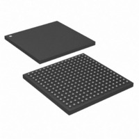
DS26324GNA3+ Maxim Integrated Products, DS26324GNA3+ Datasheet - Page 14

DS26324GNA3+
Manufacturer Part Number
DS26324GNA3+
Description
IC LIU E1/T1/J1 3.3V 256-CSBGA
Manufacturer
Maxim Integrated Products
Type
Line Interface Units (LIUs)r
Datasheet
1.DS26324GNTR.pdf
(120 pages)
Specifications of DS26324GNA3+
Number Of Drivers/receivers
16/16
Protocol
LIN
Voltage - Supply
3.135 V ~ 3.465 V
Mounting Type
Surface Mount
Package / Case
256-CSBGA
Lead Free Status / RoHS Status
Lead free / RoHS Compliant
- Current page: 14 of 120
- Download datasheet (2Mb)
SD0/RDYB/ACKB
SCLK/ALE/ASB
SDI/WRB/DSB
RDB/RWB
NAME
INTB
G14
N14
H14
C13
PIN
D7
TYPE
drain
open
O,
O
I
I
I
Shift Clock. In the serial host mode, this pin is the serial clock. Data
on SDI is clocked on the rising edge of SCLK. The data is clocked on
SDO on the rising edge of SCLK if CLKE is high. If CLKE is low the
data on SDO is clocked on the falling edge of SCLK.
Address Latch Enable. In parallel Intel multiplexed mode, the
address lines are latched on the falling edge of ALE.
Address Strobe Bar. In parallel Motorola multiplexed mode, the
address is sampled on the falling edge of ASB.
Note: Tie ALE/ASB pin high if using nonmuxed mode.
Read Bar. In Intel host mode, this pin must be low for read operation.
Read Write Bar. In Motorola mode, this pin is low for write operation
and high for read operation.
Serial Data Input. In the serial host mode, this pin is the serial input
SDI; it is sampled on the rising edge of SCLK.
Write Bar. In Intel host mode, this pin is active low during write
operation. The data or address (multiplexed mode) is sampled on the
rising edge of WRB.
Data Strobe Bar. In the parallel Motorola mode, this pin is active low.
During a write operation the data or address is sampled on the rising
edge of DSB. During a read operation the data or address is driven
on the rising edge of DSB. In the nonmultiplexed Motorola mode the
address bus (A[5:0]) is latched on the falling edge of DSB.
Serial Data Out. In serial host mode, the SDO data is output on this
pin. If a serial write is in progress this pin is high impedance. During a
read SDO is high impedance when the SDI is in command/address
mode. If CLKE is low SDO is output on the rising edge of SCLK, if
CLKE is high on the falling edge.
Ready Bar Output. A high on this pin reports to the host that the
cycle is not complete and wait states must be inserted. A low means
the cycle is complete.
Acknowledge Bar. In Motorola parallel mode, a low on this pin
indicates that the read data is available for the Host or that the written
data cycle is complete.
Interrupt Bar (Active Low). This signal is tri-state when RSTB pin is
low. This interrupt signal is driven low when an event is detected on
any of the enabled interrupt sources in any of the register banks.
When there are no active and enabled interrupt sources, the pin can
be programmed to either drive high or as open drain. The reset
default is open drain when there are no active enabled interrupt
sources. All interrupt sources are disabled when RSTB = 0 and they
must be programmed to be enabled.
DS26324 3.3V, 16-Channel, E1/T1/J1 Short-Haul Line Interface Unit
14 of 120
FUNCTION
Related parts for DS26324GNA3+
Image
Part Number
Description
Manufacturer
Datasheet
Request
R

Part Number:
Description:
IC LIU 16CH T1/E1/J1 256CSBGA
Manufacturer:
Maxim Integrated Products
Datasheet:

Part Number:
Description:
Buffers & Line Drivers 3.3V E1/T1/J1 16Ch Short Haul Octal LIU
Manufacturer:
Maxim Integrated Products

Part Number:
Description:
TYPE DS FUSED DISCONNECT SWITCH 60A 3P
Manufacturer:
EATON CUTLER HAMMER

Part Number:
Description:
MAX7528KCWPMaxim Integrated Products [CMOS Dual 8-Bit Buffered Multiplying DACs]
Manufacturer:
Maxim Integrated Products
Datasheet:

Part Number:
Description:
Single +5V, fully integrated, 1.25Gbps laser diode driver.
Manufacturer:
Maxim Integrated Products
Datasheet:

Part Number:
Description:
Single +5V, fully integrated, 155Mbps laser diode driver.
Manufacturer:
Maxim Integrated Products
Datasheet:

Part Number:
Description:
VRD11/VRD10, K8 Rev F 2/3/4-Phase PWM Controllers with Integrated Dual MOSFET Drivers
Manufacturer:
Maxim Integrated Products
Datasheet:

Part Number:
Description:
Highly Integrated Level 2 SMBus Battery Chargers
Manufacturer:
Maxim Integrated Products
Datasheet:

Part Number:
Description:
Current Monitor and Accumulator with Integrated Sense Resistor; ; Temperature Range: -40°C to +85°C
Manufacturer:
Maxim Integrated Products

Part Number:
Description:
TSSOP 14/A°/RS-485 Transceivers with Integrated 100O/120O Termination Resis
Manufacturer:
Maxim Integrated Products

Part Number:
Description:
TSSOP 14/A°/RS-485 Transceivers with Integrated 100O/120O Termination Resis
Manufacturer:
Maxim Integrated Products

Part Number:
Description:
QFN 16/A°/AC-DC and DC-DC Peak-Current-Mode Converters with Integrated Step
Manufacturer:
Maxim Integrated Products

Part Number:
Description:
TDFN/A/65V, 1A, 600KHZ, SYNCHRONOUS STEP-DOWN REGULATOR WITH INTEGRATED SWI
Manufacturer:
Maxim Integrated Products

Part Number:
Description:
Integrated Temperature Controller f
Manufacturer:
Maxim Integrated Products

Part Number:
Description:
SOT23-6/I°/45MHz to 650MHz, Integrated IF VCOs with Differential Output
Manufacturer:
Maxim Integrated Products


