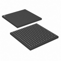
DS26324GNA3+ Maxim Integrated Products, DS26324GNA3+ Datasheet - Page 31

DS26324GNA3+
Manufacturer Part Number
DS26324GNA3+
Description
IC LIU E1/T1/J1 3.3V 256-CSBGA
Manufacturer
Maxim Integrated Products
Type
Line Interface Units (LIUs)r
Datasheet
1.DS26324GNTR.pdf
(120 pages)
Specifications of DS26324GNA3+
Number Of Drivers/receivers
16/16
Protocol
LIN
Voltage - Supply
3.135 V ~ 3.465 V
Mounting Type
Surface Mount
Package / Case
256-CSBGA
Lead Free Status / RoHS Status
Lead free / RoHS Compliant
- Current page: 31 of 120
- Download datasheet (2Mb)
5.6 Jitter Attenuator
The DS26324 contains an on-board jitter attenuator that can be set to a depth of either 32 or 128 bits via the JADS
bit in register
The 128-bit mode is used in applications where large excursions of wander are expected. The 32-bit mode is used
in delay sensitive applications. The characteristics of the attenuation are shown in
can be placed in either the receive path or the transmit path or none by appropriately setting the JAPS and the JAE
bits in register GC. These selections can be changed on an individual LIU basis by settings in the
In order for the jitter attenuator to operate properly, a 2.048MHz clock or multiple thereof, or 1.544MHz clock or
multiple thereof, must be applied at MCLK. ITU-T specification G.703 requires an accuracy of ±50ppm for both T1
and E1 applications. AT&T Pub 62411 and ANSI specs require an accuracy of ±32ppm for T1 interfaces. On-board
circuitry adjusts either the recovered clock from the clock/data recovery block or the clock applied at the TCLK pin
to create a smooth jitter-free clock, which is used to clock data out of the jitter attenuator FIFO. It is acceptable to
provide a jittery clock at the TCLK pin if the jitter attenuator is placed on the transmit side. If the incoming jitter
exceeds either 120UI
internal nominal 32.768MHz (E1) or 24.704MHz (T1) clock by either 15 or 17 instead of the normal 16 to keep the
buffer from overflowing. When the device divides by either 15 or 17, it also sets the jitter attenuator limit trip
(IJAFLT) bits in the
Figure 5-9. Jitter Attenuation
GC.
It can also be controlled on an individual LIU basis by settings in the
IJAFLT
-20dB
-40dB
-60dB
P-P
0dB
(buffer depth is 128 bits) or 28UI
register described.
1
10
E1
DS26324 3.3V, 16-Channel, E1/T1/J1 Short-Haul Line Interface Unit
Prohibited
TBR12
Area
T1
31 of 120
100
FREQUENCY (Hz)
P-P
(buffer depth is 32 bits), the DS26324 will divide the
1K
Prohibited Area
ITU G.7XX
TR 62411 (Dec. 90)
Prohibited Area
10K
Figure
IJAFDS
5-9. The jitter attenuator
100K
register.
IJAPS
and IJAE.
Related parts for DS26324GNA3+
Image
Part Number
Description
Manufacturer
Datasheet
Request
R

Part Number:
Description:
IC LIU 16CH T1/E1/J1 256CSBGA
Manufacturer:
Maxim Integrated Products
Datasheet:

Part Number:
Description:
Buffers & Line Drivers 3.3V E1/T1/J1 16Ch Short Haul Octal LIU
Manufacturer:
Maxim Integrated Products

Part Number:
Description:
TYPE DS FUSED DISCONNECT SWITCH 60A 3P
Manufacturer:
EATON CUTLER HAMMER

Part Number:
Description:
MAX7528KCWPMaxim Integrated Products [CMOS Dual 8-Bit Buffered Multiplying DACs]
Manufacturer:
Maxim Integrated Products
Datasheet:

Part Number:
Description:
Single +5V, fully integrated, 1.25Gbps laser diode driver.
Manufacturer:
Maxim Integrated Products
Datasheet:

Part Number:
Description:
Single +5V, fully integrated, 155Mbps laser diode driver.
Manufacturer:
Maxim Integrated Products
Datasheet:

Part Number:
Description:
VRD11/VRD10, K8 Rev F 2/3/4-Phase PWM Controllers with Integrated Dual MOSFET Drivers
Manufacturer:
Maxim Integrated Products
Datasheet:

Part Number:
Description:
Highly Integrated Level 2 SMBus Battery Chargers
Manufacturer:
Maxim Integrated Products
Datasheet:

Part Number:
Description:
Current Monitor and Accumulator with Integrated Sense Resistor; ; Temperature Range: -40°C to +85°C
Manufacturer:
Maxim Integrated Products

Part Number:
Description:
TSSOP 14/A°/RS-485 Transceivers with Integrated 100O/120O Termination Resis
Manufacturer:
Maxim Integrated Products

Part Number:
Description:
TSSOP 14/A°/RS-485 Transceivers with Integrated 100O/120O Termination Resis
Manufacturer:
Maxim Integrated Products

Part Number:
Description:
QFN 16/A°/AC-DC and DC-DC Peak-Current-Mode Converters with Integrated Step
Manufacturer:
Maxim Integrated Products

Part Number:
Description:
TDFN/A/65V, 1A, 600KHZ, SYNCHRONOUS STEP-DOWN REGULATOR WITH INTEGRATED SWI
Manufacturer:
Maxim Integrated Products

Part Number:
Description:
Integrated Temperature Controller f
Manufacturer:
Maxim Integrated Products

Part Number:
Description:
SOT23-6/I°/45MHz to 650MHz, Integrated IF VCOs with Differential Output
Manufacturer:
Maxim Integrated Products


