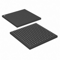
DS26324GNA3+ Maxim Integrated Products, DS26324GNA3+ Datasheet - Page 91

DS26324GNA3+
Manufacturer Part Number
DS26324GNA3+
Description
IC LIU E1/T1/J1 3.3V 256-CSBGA
Manufacturer
Maxim Integrated Products
Type
Line Interface Units (LIUs)r
Datasheet
1.DS26324GNTR.pdf
(120 pages)
Specifications of DS26324GNA3+
Number Of Drivers/receivers
16/16
Protocol
LIN
Voltage - Supply
3.135 V ~ 3.465 V
Mounting Type
Surface Mount
Package / Case
256-CSBGA
Lead Free Status / RoHS Status
Lead free / RoHS Compliant
- Current page: 91 of 120
- Download datasheet (2Mb)
7 JTAG BOUNDARY SCAN ARCHITECTURE AND TEST ACCESS PORT
The DS26324 IEEE 1149.1 design supports the standard instruction codes SAMPLE/PRELOAD, BYPASS, and
EXTEST. Optional public instructions included are HIGHZ, CLAMP, and IDCODE. The DS26324 contains the
following as required by IEEE 1149.1 Standard Test-Access Port and Boundary-Scan Architecture:
Details on Boundary Scan Architecture and the Test Access Port can be found in IEEE 1149.1-1990, IEEE
1149.1a-1993, and IEEE 1149.1b-1994. The Test Access Port has the necessary interface pins: TRSTB, TCLK,
TMS,
go to
Figure 7-1. JTAG Functional Block Diagram
www.maxim-ic.com/tools/bsdl/
Test Access Port (TAP)
TAP Controller
Instruction Register
TDI,
and
10kΩ
TDO.
+V
TDI
See
10kΩ
+V
and search for DS26324.
the
TMS
pin
TEST ACCESS PORT
BOUNDARY SCAN
DS26324 3.3V, 16-Channel, E1/T1/J1 Short-Haul Line Interface Unit
INDENTIFICATION
CONTROLLER
INSTRUCTION
REGISTER
REGISTER
REGISTER
REGISTER
descriptions
BYPASS
TCLK
91 of 120
10kΩ
+V
TRSTB
for
SELECT
OUTPUT ENABLE
Bypass Register
Boundary Scan Register
Device Identification Register
details.
MUX
For
the
TDO
latest
BSDL
files
Related parts for DS26324GNA3+
Image
Part Number
Description
Manufacturer
Datasheet
Request
R

Part Number:
Description:
IC LIU 16CH T1/E1/J1 256CSBGA
Manufacturer:
Maxim Integrated Products
Datasheet:

Part Number:
Description:
Buffers & Line Drivers 3.3V E1/T1/J1 16Ch Short Haul Octal LIU
Manufacturer:
Maxim Integrated Products

Part Number:
Description:
TYPE DS FUSED DISCONNECT SWITCH 60A 3P
Manufacturer:
EATON CUTLER HAMMER

Part Number:
Description:
MAX7528KCWPMaxim Integrated Products [CMOS Dual 8-Bit Buffered Multiplying DACs]
Manufacturer:
Maxim Integrated Products
Datasheet:

Part Number:
Description:
Single +5V, fully integrated, 1.25Gbps laser diode driver.
Manufacturer:
Maxim Integrated Products
Datasheet:

Part Number:
Description:
Single +5V, fully integrated, 155Mbps laser diode driver.
Manufacturer:
Maxim Integrated Products
Datasheet:

Part Number:
Description:
VRD11/VRD10, K8 Rev F 2/3/4-Phase PWM Controllers with Integrated Dual MOSFET Drivers
Manufacturer:
Maxim Integrated Products
Datasheet:

Part Number:
Description:
Highly Integrated Level 2 SMBus Battery Chargers
Manufacturer:
Maxim Integrated Products
Datasheet:

Part Number:
Description:
Current Monitor and Accumulator with Integrated Sense Resistor; ; Temperature Range: -40°C to +85°C
Manufacturer:
Maxim Integrated Products

Part Number:
Description:
TSSOP 14/A°/RS-485 Transceivers with Integrated 100O/120O Termination Resis
Manufacturer:
Maxim Integrated Products

Part Number:
Description:
TSSOP 14/A°/RS-485 Transceivers with Integrated 100O/120O Termination Resis
Manufacturer:
Maxim Integrated Products

Part Number:
Description:
QFN 16/A°/AC-DC and DC-DC Peak-Current-Mode Converters with Integrated Step
Manufacturer:
Maxim Integrated Products

Part Number:
Description:
TDFN/A/65V, 1A, 600KHZ, SYNCHRONOUS STEP-DOWN REGULATOR WITH INTEGRATED SWI
Manufacturer:
Maxim Integrated Products

Part Number:
Description:
Integrated Temperature Controller f
Manufacturer:
Maxim Integrated Products

Part Number:
Description:
SOT23-6/I°/45MHz to 650MHz, Integrated IF VCOs with Differential Output
Manufacturer:
Maxim Integrated Products


