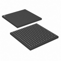
DS26324GNA3+ Maxim Integrated Products, DS26324GNA3+ Datasheet - Page 56

DS26324GNA3+
Manufacturer Part Number
DS26324GNA3+
Description
IC LIU E1/T1/J1 3.3V 256-CSBGA
Manufacturer
Maxim Integrated Products
Type
Line Interface Units (LIUs)r
Datasheet
1.DS26324GNTR.pdf
(120 pages)
Specifications of DS26324GNA3+
Number Of Drivers/receivers
16/16
Protocol
LIN
Voltage - Supply
3.135 V ~ 3.465 V
Mounting Type
Surface Mount
Package / Case
256-CSBGA
Lead Free Status / RoHS Status
Lead free / RoHS Compliant
Register Name:
Register Description:
Register Address (LIUs 1–8):
Bit #
Name
Default
Note: CRIMP controls all 16 LIUs. All other bits are for LIUs 1–8 only.
Bit 7: Receive Impedance Mode Select (RIMPMS). When this bit is set, fully internal impedance match mode is
selected, so RTIP and RRING require no external resistor. If this bit is set, the receiver line transformer must be a
1:1 turns ratio and the RTR bit set. When reset, external termination mode is selected and an external resistor is
required to terminate the receive line. This external resistor will be adjusted internally to the correct termination
value if partially internal impedance matching is turned on (TS.RIMPON = 1).
Bit 6: AIS Enable During Loss (AISEL). When this bit is set, an AIS is sent to the system side upon detecting
LOS for each channel. The individual LIU register
the
Bit 5: Short Circuit Protection Disable (SCPD). If this bit is set the short-circuit protection is disabled for all the
transmitters. The individual LIU register
register will have control.
Bit 4: Code (CODE). If this bit is set AMI encoder/decoder is selected. The
when this bit is set. If reset, the
Bit 3: Jitter Attenuator Depth Select (JADS). If this bit is set the jitter attenuator FIFO depth is 128 bits. The
settings in the
Bit 2: Calibrate Receive Internal Termination (CRIMP). A low-to-high transition on this bit initiates a calibration
cycle for the receive internal termination. This requires a 16kΩ ±1% resistor on the RESREF pin. Bit 2 of the GC
register at address 0x2F must also be set to enable calibration. While this bit is set, RSL4.4 (0x0F in individual
bank) will indicate the status of the calibration cycle.
Bit 1: Jitter Attenuator Position Select (JAPS). When the JAPS bit is set high, the jitter attenuator will be in the
receive path and when default or set low in the Transmit path. These settings can be changed for an individual LIU
by settings in the
Bit 0: Jitter Attenuator Enable (JAE). When this bit is set the jitter attenuator is enabled. The settings in the
register will be ignored if this register is set. If reset, the IJAE register will have control.
IAISEL
register will have control.
RIMPMS
IJAFDS
7
0
IJAPS
register will be ignored if this register is set. If reset the
register. Note that when bit JAE is set, the settings in the
AISEL
6
0
LCS
GC
Global Configuration
0Fh
register will have control.
SCPD
ISCPD
5
0
DS26324 3.3V, 16-Channel, E1/T1/J1 Short-Haul Line Interface Unit
settings will be ignored when this bit is set. When reset, the
IAISEL
CODE
56 of 120
4
0
settings will be ignored when this bit is set. When reset,
JADS
3
0
CRIMP
LCS
IJAFDS
2
0
IJAPS
register settings will be ignored
register will have control.
register will be ignored.
JAPS
1
0
JAE
0
0
ISCPD
IJAE


