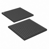
DS26324GNA3+ Maxim Integrated Products, DS26324GNA3+ Datasheet - Page 69

DS26324GNA3+
Manufacturer Part Number
DS26324GNA3+
Description
IC LIU E1/T1/J1 3.3V 256-CSBGA
Manufacturer
Maxim Integrated Products
Type
Line Interface Units (LIUs)r
Datasheet
1.DS26324GNTR.pdf
(120 pages)
Specifications of DS26324GNA3+
Number Of Drivers/receivers
16/16
Protocol
LIN
Voltage - Supply
3.135 V ~ 3.465 V
Mounting Type
Surface Mount
Package / Case
256-CSBGA
Lead Free Status / RoHS Status
Lead free / RoHS Compliant
- Current page: 69 of 120
- Download datasheet (2Mb)
Register Name:
Register Description:
Register Address:
Bit #
Name
Default
Bits 7 and 6: PLL Clock Input [1:0] (PCLKI[1:0]). These bits select the input into to the PLL.
Bit 5: T1/E1 Clock Enable (TECLKE). When this bit is set the TECLK output is enabled. If not set TECLK will be
disabled and the TECLK output is a LOS output. TECLK requires PLLE to be set for correct functionality.
Bit 4: Clock A Enable (CLKAE). When this bit is set the CLKA output is enabled. If not set CLKA will be disabled
and the CLKA output is a LOS output. CLKA requires PLLE to be set for correct functionality.
Bits 3 and 2: Master Period Select [1:0] (MPS[1:0]). These bits MPS[1:0] selects the external MCLK frequency
for the DS26324. See
Channels 9 to 16.
Bit 1: Frequency Select (FREQS). In conjunction with MPS[1:0] selects the external MCLK frequency for the
DS26324. If this bit is set the external Master clock can be 1.544MHz or multiple thereof. If not set the external
master clock can be 2.048MHz or multiple thereof. See
controller functionality of Channels 9 to 16.
Bit 0: Phase Lock Loop Enable (PLLE). When this bit is set the phase lock loop is enabled. If not set MCLK will
be the applied input clock.
Table 6-15. DS26324 MCLK Selections
PLLE
0
0
1
1
1
1
1
1
1
1
PCLKI1
MPS1, MPS0
7
0
00: MCLK is used.
01: RCLK1 to 8 is used based on the selection in register
10: RCLK9 to 16 is used based on the selection in register CCR.
11: Reserved.
xx
xx
00
01
10
11
00
01
10
11
Table 6-15
PCLKI0
6
0
MHz ±50ppm
MC
Master Clock Select
06h
MCLK,
12.352
16.384
1.544
2.048
1.544
3.088
6.176
2.048
4.096
8.192
for details. This register when written to will also controller functionality of
TECLKE
5
0
DS26324 3.3V, 16-Channel, E1/T1/J1 Short-Haul Line Interface Unit
FREQS
CLKAE
69 of 120
x
x
1
1
1
1
0
0
0
0
4
0
Table 6-15
MPS1
T1/J1 or E1
T1/J1 or E1
T1/J1 or E1
T1/J1 or E1
T1/J1 or E1
T1/J1 or E1
T1/J1 or E1
T1/J1 or E1
for details. This register when written to will also
3
0
MODE
T1
E1
CCR.
MPS0
2
0
FREQS
1
0
PLLE
0
0
Related parts for DS26324GNA3+
Image
Part Number
Description
Manufacturer
Datasheet
Request
R

Part Number:
Description:
IC LIU 16CH T1/E1/J1 256CSBGA
Manufacturer:
Maxim Integrated Products
Datasheet:

Part Number:
Description:
Buffers & Line Drivers 3.3V E1/T1/J1 16Ch Short Haul Octal LIU
Manufacturer:
Maxim Integrated Products

Part Number:
Description:
TYPE DS FUSED DISCONNECT SWITCH 60A 3P
Manufacturer:
EATON CUTLER HAMMER

Part Number:
Description:
MAX7528KCWPMaxim Integrated Products [CMOS Dual 8-Bit Buffered Multiplying DACs]
Manufacturer:
Maxim Integrated Products
Datasheet:

Part Number:
Description:
Single +5V, fully integrated, 1.25Gbps laser diode driver.
Manufacturer:
Maxim Integrated Products
Datasheet:

Part Number:
Description:
Single +5V, fully integrated, 155Mbps laser diode driver.
Manufacturer:
Maxim Integrated Products
Datasheet:

Part Number:
Description:
VRD11/VRD10, K8 Rev F 2/3/4-Phase PWM Controllers with Integrated Dual MOSFET Drivers
Manufacturer:
Maxim Integrated Products
Datasheet:

Part Number:
Description:
Highly Integrated Level 2 SMBus Battery Chargers
Manufacturer:
Maxim Integrated Products
Datasheet:

Part Number:
Description:
Current Monitor and Accumulator with Integrated Sense Resistor; ; Temperature Range: -40°C to +85°C
Manufacturer:
Maxim Integrated Products

Part Number:
Description:
TSSOP 14/A°/RS-485 Transceivers with Integrated 100O/120O Termination Resis
Manufacturer:
Maxim Integrated Products

Part Number:
Description:
TSSOP 14/A°/RS-485 Transceivers with Integrated 100O/120O Termination Resis
Manufacturer:
Maxim Integrated Products

Part Number:
Description:
QFN 16/A°/AC-DC and DC-DC Peak-Current-Mode Converters with Integrated Step
Manufacturer:
Maxim Integrated Products

Part Number:
Description:
TDFN/A/65V, 1A, 600KHZ, SYNCHRONOUS STEP-DOWN REGULATOR WITH INTEGRATED SWI
Manufacturer:
Maxim Integrated Products

Part Number:
Description:
Integrated Temperature Controller f
Manufacturer:
Maxim Integrated Products

Part Number:
Description:
SOT23-6/I°/45MHz to 650MHz, Integrated IF VCOs with Differential Output
Manufacturer:
Maxim Integrated Products


