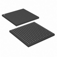
DS26324GNA3+ Maxim Integrated Products, DS26324GNA3+ Datasheet - Page 19

DS26324GNA3+
Manufacturer Part Number
DS26324GNA3+
Description
IC LIU E1/T1/J1 3.3V 256-CSBGA
Manufacturer
Maxim Integrated Products
Type
Line Interface Units (LIUs)r
Datasheet
1.DS26324GNTR.pdf
(120 pages)
Specifications of DS26324GNA3+
Number Of Drivers/receivers
16/16
Protocol
LIN
Voltage - Supply
3.135 V ~ 3.465 V
Mounting Type
Surface Mount
Package / Case
256-CSBGA
Lead Free Status / RoHS Status
Lead free / RoHS Compliant
- Current page: 19 of 120
- Download datasheet (2Mb)
DS26324 3.3V, 16-Channel, E1/T1/J1 Short-Haul Line Interface Unit
Figure 5-4. Interrupt Handling Flow Diagram
Interrupt Allowed
No
Interrupt Conditon
Exist?
Yes
Read Interrupt Status
Register
Read Corresponding Status
Register (Optional)
Service the Interrupt
5.2 Power-Up and Reset
Internal Power_On_Reset circuitry generates a reset during power-up. All registers are reset to the default values.
Writing to the Software Reset Register generates at least 1µs reset cycle, which has the same effect as the power-
up reset.
The DS26324 can be reset by a low going pulse on the RSTB pin (see
Table
4-1). A reset can also be performed in
software by writing any value to the
SWR
register.
5.3 Master Clock
The DS26324 requires 2.048MHz ±50ppm or 1.544MHz ±50ppm or multiple thereof. The receiver uses the MCLK
as a reference for clock recovery, jitter attenuation and generating RCLK during LOS. The AIS tTransmission uses
MCLK for transmit all ones condition. See register
MC
to set desired incoming frequency. When the PLLE bit is set,
the master clock adapter will generate both 2.048MHz (E1) and 1.544MHz (T1) clocks. If the PLLE bit is clear, both
internal reference clocks will track MCLK.
MCLK or RCLK can also be used to output CLKA on the LOS16 pin. Register
CCR
is used to select the clock
generated for CLKA and the TECLK. Any RCLK can also be selected as an input to the clock generator using this
same register. For a detailed description of selections available see
Figure
5-5.
19 of 120
Related parts for DS26324GNA3+
Image
Part Number
Description
Manufacturer
Datasheet
Request
R

Part Number:
Description:
IC LIU 16CH T1/E1/J1 256CSBGA
Manufacturer:
Maxim Integrated Products
Datasheet:

Part Number:
Description:
Buffers & Line Drivers 3.3V E1/T1/J1 16Ch Short Haul Octal LIU
Manufacturer:
Maxim Integrated Products

Part Number:
Description:
TYPE DS FUSED DISCONNECT SWITCH 60A 3P
Manufacturer:
EATON CUTLER HAMMER

Part Number:
Description:
MAX7528KCWPMaxim Integrated Products [CMOS Dual 8-Bit Buffered Multiplying DACs]
Manufacturer:
Maxim Integrated Products
Datasheet:

Part Number:
Description:
Single +5V, fully integrated, 1.25Gbps laser diode driver.
Manufacturer:
Maxim Integrated Products
Datasheet:

Part Number:
Description:
Single +5V, fully integrated, 155Mbps laser diode driver.
Manufacturer:
Maxim Integrated Products
Datasheet:

Part Number:
Description:
VRD11/VRD10, K8 Rev F 2/3/4-Phase PWM Controllers with Integrated Dual MOSFET Drivers
Manufacturer:
Maxim Integrated Products
Datasheet:

Part Number:
Description:
Highly Integrated Level 2 SMBus Battery Chargers
Manufacturer:
Maxim Integrated Products
Datasheet:

Part Number:
Description:
Current Monitor and Accumulator with Integrated Sense Resistor; ; Temperature Range: -40°C to +85°C
Manufacturer:
Maxim Integrated Products

Part Number:
Description:
TSSOP 14/A°/RS-485 Transceivers with Integrated 100O/120O Termination Resis
Manufacturer:
Maxim Integrated Products

Part Number:
Description:
TSSOP 14/A°/RS-485 Transceivers with Integrated 100O/120O Termination Resis
Manufacturer:
Maxim Integrated Products

Part Number:
Description:
QFN 16/A°/AC-DC and DC-DC Peak-Current-Mode Converters with Integrated Step
Manufacturer:
Maxim Integrated Products

Part Number:
Description:
TDFN/A/65V, 1A, 600KHZ, SYNCHRONOUS STEP-DOWN REGULATOR WITH INTEGRATED SWI
Manufacturer:
Maxim Integrated Products

Part Number:
Description:
Integrated Temperature Controller f
Manufacturer:
Maxim Integrated Products

Part Number:
Description:
SOT23-6/I°/45MHz to 650MHz, Integrated IF VCOs with Differential Output
Manufacturer:
Maxim Integrated Products


