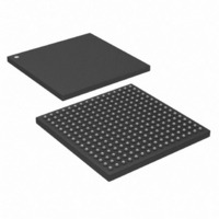
DS26324GNA3+ Maxim Integrated Products, DS26324GNA3+ Datasheet - Page 84

DS26324GNA3+
Manufacturer Part Number
DS26324GNA3+
Description
IC LIU E1/T1/J1 3.3V 256-CSBGA
Manufacturer
Maxim Integrated Products
Type
Line Interface Units (LIUs)r
Datasheet
1.DS26324GNTR.pdf
(120 pages)
Specifications of DS26324GNA3+
Number Of Drivers/receivers
16/16
Protocol
LIN
Voltage - Supply
3.135 V ~ 3.465 V
Mounting Type
Surface Mount
Package / Case
256-CSBGA
Lead Free Status / RoHS Status
Lead free / RoHS Compliant
6.1.4 BERT Registers
Register Name:
Register Description:
Register Address (LIUs 1–8):
Register Address (LIUs 9–16):
Bit #
Name
Default
Bit 7: Performance Monitoring Update Mode (PMUM). When 0, a performance monitoring update is initiated by
the LPMU register bit. When 1, a performance monitoring update is initiated by the receive performance monitoring
update signal (RPMU). Note: If RPMU or LPMU is one, changing the state of this bit may cause a performance
monitoring update to occur.
Bit 6: Local Performance Monitoring Update (LPMU). This bit causes a performance monitoring update to be
initiated if local performance monitoring update is enabled (PMUM = 0). A 0-to-1 transition causes the performance
monitoring registers to be updated with the latest data, and the counters reset (0 or 1). For a second performance
monitoring update to be initiated, this bit must be set to 0, and back to 1. If LPMU goes low before the PMS bit
goes high, an update might not be performed. This bit has no affect when PMUM = 1.
Bit 5: Receive New Pattern Load (RNPL). A 0-to-1 transition of this bit will cause the programmed test pattern
(QRSS, PTS, PLF[4:0], PTF[4:0], and BSP[31:0]) to be loaded in to the receive pattern generator. This bit must be
changed to zero and back to one for another pattern to be loaded. Loading a new pattern will forces the receive
pattern generator out of the “Sync” state which causes a resynchronization to be initiated. Note: QRSS, PTS,
PLF[4:0], PTF[4:0], and BSP[31:0] must not change from the time this bit transitions from 0 to 1 until four RXCK
clock cycles after this bit transitions from 0 to 1.
Bit 4: Receive Pattern Inversion Control (RPIC). When 0, the receive incoming data stream is not altered. When
1, the receive incoming data stream is inverted.
Bit 3: Manual Pattern Resynchronization (MPR). A zero to one transition of this bit will cause the receive pattern
generator to resynchronize to the incoming pattern. This bit must be changed to zero and back to one for another
resynchronization to be initiated. Note: A manual resynchronization forces the receive pattern generator out of the
“Sync” state.
Bit 2: Automatic Pattern Resynchronization Disable (APRD). When 0, the receive pattern generator will
automatically resynchronize to the incoming pattern if six or more times during the current 64-bit window the
incoming data stream bit and the receive pattern generator output bit did not match. When 1, the receive pattern
generator will not automatically resynchronize to the incoming pattern. Note: Automatic synchronization is
prevented by not allowing the receive pattern generator to automatically exit the “Sync” state.
Bit 1: Transmit New Pattern Load (TNPL). A 0-to-1 transition of this bit will cause the programmed test pattern
(QRSS, PTS, PLF[4:0], PTF[4:0], and BSP[31:0]) to be loaded in to the transmit pattern generator. This bit must be
changed to zero and back to one for another pattern to be loaded. Note: QRSS, PTS, PLF[4:0], PTF[4:0], and
BSP[31:0] must not change from the time this bit transitions from 0 to 1 until four TXCK clock cycles after this bit
transitions from 0 to 1.
Bit 0: Transmit Pattern Inversion Control (TPIC). When 0, the transmit outgoing data stream is not altered.
When 1, the transmit outgoing data stream is inverted.
PMUM
7
0
LPMU
6
0
BCR
BERT Control
00h
20h
RNPL
5
0
DS26324 3.3V, 16-Channel, E1/T1/J1 Short-Haul Line Interface Unit
84 of 120
RPIC
4
0
MPR
3
0
APRD
2
0
TNPL
1
0
TPIC
0
0


