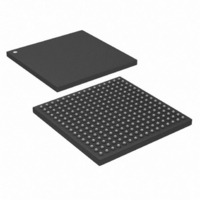
DS26324GNA3+ Maxim Integrated Products, DS26324GNA3+ Datasheet - Page 15

DS26324GNA3+
Manufacturer Part Number
DS26324GNA3+
Description
IC LIU E1/T1/J1 3.3V 256-CSBGA
Manufacturer
Maxim Integrated Products
Type
Line Interface Units (LIUs)r
Datasheet
1.DS26324GNTR.pdf
(120 pages)
Specifications of DS26324GNA3+
Number Of Drivers/receivers
16/16
Protocol
LIN
Voltage - Supply
3.135 V ~ 3.465 V
Mounting Type
Surface Mount
Package / Case
256-CSBGA
Lead Free Status / RoHS Status
Lead free / RoHS Compliant
- Current page: 15 of 120
- Download datasheet (2Mb)
CLKE/MUX
A5/BSWP
D7/AD7
D6/AD6
D5/AD5
D4/AD4
D3/AD3
D2/AD2
D1/AD1
D0/AD0
TRSTB
NAME
TMS
TDO
TCK
TDI
OE
A4
A3
A2
A1
A0
N10
R12
T14
E15
B13
D14
A15
B15
PIN
M4
M5
N3
C4
H5
G3
H3
P3
L5
K7
P4
L6
E4
tri-state
high-Z
TYPE
pullup
pullup
pullup
I/O,
O,
I,
I,
I,
I
I
I
I
I
Data Bus 7–0. In nonmultiplexed host mode, these pins are the
bidirectional data bus.
Address/Data Bus 7–0. In multiplexed host mode, these pins are the
bidirectional address/data bus. Note: AD7 and AD6 do not carry
address information.
In serial host mode, these pins should be grounded.
Address 5. In the host nonmultiplexed mode, this is the most
significant bit of the address bus.
Bit Swap. In serial host mode, this bit defines the serial data position
to be MSB first when low and LSB first when high.
In multiplexed host mode, this pin should be grounded.
Address Bus 4–0. These five pins are address pins in the parallel
host mode.
In serial host mode and multiplexed host mode, these pins should be
grounded.
Output Enable. If this pin is pulled low all the transmitters outputs
(TTIP and TRING) are high impedance. If pulled high all the
transmitters are enabled when the associated output enable
set. If TST.RHPMC is set, the OE pin is granted control of the
receiver internal termination. When OE is low, receiver internal
termination will be high impedance. When OE is high, receiver
termination will be enabled. The receiver can still monitor incoming
signals even when termination is in high impedance.
Clock Edge. If CLKE is high, SDO is clocked out on falling edge of
SCLK and if low SDO is on rising edge of SCLK.
Multiplexed/Nonmultiplexed Select Pin. When in parallel port
mode, this pin is used to select multiplexed address and data
operation or separate address and data. When mux is a high
multiplexed address and data is used and when mux is low
nonmultiplexed is used.
JTAG Test Port Reset. This pin if low will reset the JTAG port. If not
used it can be left unconnected.
JTAG Test Mode Select. This pin is clocked on the rising edge of
TCK and is used to control the JTAG selection between scan and
Test Machine control.
JTAG Test Clock. The data TDI and TMS are clocked on rising edge
of TCK and TDO is clocked out on the falling edge of TCK.
JTAG Test Data Out. This is the serial output of the JTAG port. The
data is clocked out on the falling edge of TCK.
Test Data Input. This pin input is the serial data of the JTAG Test.
The data on TDI is clocked on the rising edge of TCK. This pin can be
left unconnected.
DS26324 3.3V, 16-Channel, E1/T1/J1 Short-Haul Line Interface Unit
15 of 120
JTAG
FUNCTION
OE
bit is
Related parts for DS26324GNA3+
Image
Part Number
Description
Manufacturer
Datasheet
Request
R

Part Number:
Description:
IC LIU 16CH T1/E1/J1 256CSBGA
Manufacturer:
Maxim Integrated Products
Datasheet:

Part Number:
Description:
Buffers & Line Drivers 3.3V E1/T1/J1 16Ch Short Haul Octal LIU
Manufacturer:
Maxim Integrated Products

Part Number:
Description:
TYPE DS FUSED DISCONNECT SWITCH 60A 3P
Manufacturer:
EATON CUTLER HAMMER

Part Number:
Description:
MAX7528KCWPMaxim Integrated Products [CMOS Dual 8-Bit Buffered Multiplying DACs]
Manufacturer:
Maxim Integrated Products
Datasheet:

Part Number:
Description:
Single +5V, fully integrated, 1.25Gbps laser diode driver.
Manufacturer:
Maxim Integrated Products
Datasheet:

Part Number:
Description:
Single +5V, fully integrated, 155Mbps laser diode driver.
Manufacturer:
Maxim Integrated Products
Datasheet:

Part Number:
Description:
VRD11/VRD10, K8 Rev F 2/3/4-Phase PWM Controllers with Integrated Dual MOSFET Drivers
Manufacturer:
Maxim Integrated Products
Datasheet:

Part Number:
Description:
Highly Integrated Level 2 SMBus Battery Chargers
Manufacturer:
Maxim Integrated Products
Datasheet:

Part Number:
Description:
Current Monitor and Accumulator with Integrated Sense Resistor; ; Temperature Range: -40°C to +85°C
Manufacturer:
Maxim Integrated Products

Part Number:
Description:
TSSOP 14/A°/RS-485 Transceivers with Integrated 100O/120O Termination Resis
Manufacturer:
Maxim Integrated Products

Part Number:
Description:
TSSOP 14/A°/RS-485 Transceivers with Integrated 100O/120O Termination Resis
Manufacturer:
Maxim Integrated Products

Part Number:
Description:
QFN 16/A°/AC-DC and DC-DC Peak-Current-Mode Converters with Integrated Step
Manufacturer:
Maxim Integrated Products

Part Number:
Description:
TDFN/A/65V, 1A, 600KHZ, SYNCHRONOUS STEP-DOWN REGULATOR WITH INTEGRATED SWI
Manufacturer:
Maxim Integrated Products

Part Number:
Description:
Integrated Temperature Controller f
Manufacturer:
Maxim Integrated Products

Part Number:
Description:
SOT23-6/I°/45MHz to 650MHz, Integrated IF VCOs with Differential Output
Manufacturer:
Maxim Integrated Products


