C8051F120DK Silicon Laboratories Inc, C8051F120DK Datasheet - Page 182
C8051F120DK
Manufacturer Part Number
C8051F120DK
Description
DEVKIT-F120/21/22/23/24/25/26/27
Manufacturer
Silicon Laboratories Inc
Type
MCUr
Datasheet
1.C8051F120DK.pdf
(350 pages)
Specifications of C8051F120DK
Contents
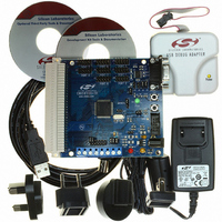
Evaluation Board, Power Supply, USB Cables, Adapter and Documentation
Processor To Be Evaluated
C8051F12x and C8051F13x
Interface Type
USB
Silicon Manufacturer
Silicon Labs
Core Architecture
8051
Silicon Core Number
C8051F120
Silicon Family Name
C8051F12x
Lead Free Status / RoHS Status
Contains lead / RoHS non-compliant
For Use With/related Products
C8051F120, 121, 122, 123, 124, 125, 126, 127
Lead Free Status / Rohs Status
Lead free / RoHS Compliant
Other names
336-1224
Available stocks
Company
Part Number
Manufacturer
Quantity
Price
Company:

Part Number:
C8051F120DK
Manufacturer:
SiliconL
Quantity:
4


C8051F120/1/2/3/4/5/6/7
C8051F130/1/2/3
182
Bit7:
Bit6:
Bit5:
Bit4:
Bit3:
Bit2:
Bit1:
Bit0:
Bit7
R
-
Reserved.
CNVRSEF: Convert Start 0 Reset Source Enable and Flag
Write:
Read:
C0RSEF: Comparator0 Reset Enable and Flag.
Write:
Read:
SWRSF: Software Reset Force and Flag.
Write:
Read:
WDTRSF: Watchdog Timer Reset Flag.
MCDRSF: Missing Clock Detector Flag.
Write:
Read:
PORSF: Power-On Reset Flag.
Write: If the V
be written to select or de-select the V
0: De-select the V
1: Select the V
Important: At power-on, the V
enable pin (MONEN). The PORSF bit does not disable or enable the V
ply selects the V
Read: This bit is set whenever a power-on reset occurs. This may be due to a true power-on reset or a
V
reset.
0: Source of last reset was not a power-on or V
1: Source of last reset was a power-on or V
Note: When this flag is read as '1', all other reset flags are indeterminate.
PINRSF: HW Pin Reset Flag.
Write:
Read:
DD
CNVRSEF C0RSEF SWRSEF WDTRSF MCDRSF
monitor reset. In either case, data memory should be considered indeterminate following the
R/W
Bit6
0: CNVSTR0 is not a reset source.
1: CNVSTR0 is a reset source (active low).
0: Source of prior reset was not CNVSTR0.
1: Source of prior reset was CNVSTR0.
0: Comparator0 is not a reset source.
1: Comparator0 is a reset source (active low).
0: Source of last reset was not Comparator0.
1: Source of last reset was Comparator0.
0: No effect.
1: Forces an internal reset. RST pin is not effected.
0: Source of last reset was not a write to the SWRSF bit.
1: Source of last reset was a write to the SWRSF bit.
0: Source of last reset was not WDT timeout.
1: Source of last reset was WDT timeout.
0: Missing Clock Detector disabled.
1: Missing Clock Detector enabled; triggers a reset if a missing clock condition is detected.
0: Source of last reset was not a Missing Clock Detector timeout.
1: Source of last reset was a Missing Clock Detector timeout.
0: No effect.
1: Forces a Power-On Reset. RST is driven low.
0: Source of prior reset was not RST pin.
1: Source of prior reset was RST pin.
SFR Definition 13.2. RSTSRC: Reset Source
DD
DD
monitor circuitry is enabled (by tying the MONEN pin to a logic high state), this bit can
DD
DD
monitor as a reset source.
R/W
Bit5
monitor as a reset source.
monitor as a reset source.
R/W
Bit4
DD
monitor is enabled/disabled using the external V
DD
Rev. 1.4
monitor as a reset source.
DD
Bit3
R
monitor reset.
DD
monitor reset.
R/W
Bit2
PORSF
R/W
Bit1
DD
SFR Address:
monitor circuit. It sim-
PINRSF
SFR Page:
R/W
Bit0
DD
monitor
0xEF
0
00000000
Reset Value
Related parts for C8051F120DK
Image
Part Number
Description
Manufacturer
Datasheet
Request
R

Part Number:
Description:
SMD/C°/SINGLE-ENDED OUTPUT SILICON OSCILLATOR
Manufacturer:
Silicon Laboratories Inc
Part Number:
Description:
Manufacturer:
Silicon Laboratories Inc
Datasheet:
Part Number:
Description:
N/A N/A/SI4010 AES KEYFOB DEMO WITH LCD RX
Manufacturer:
Silicon Laboratories Inc
Datasheet:
Part Number:
Description:
N/A N/A/SI4010 SIMPLIFIED KEY FOB DEMO WITH LED RX
Manufacturer:
Silicon Laboratories Inc
Datasheet:
Part Number:
Description:
N/A/-40 TO 85 OC/EZLINK MODULE; F930/4432 HIGH BAND (REV E/B1)
Manufacturer:
Silicon Laboratories Inc
Part Number:
Description:
EZLink Module; F930/4432 Low Band (rev e/B1)
Manufacturer:
Silicon Laboratories Inc
Part Number:
Description:
I°/4460 10 DBM RADIO TEST CARD 434 MHZ
Manufacturer:
Silicon Laboratories Inc
Part Number:
Description:
I°/4461 14 DBM RADIO TEST CARD 868 MHZ
Manufacturer:
Silicon Laboratories Inc
Part Number:
Description:
I°/4463 20 DBM RFSWITCH RADIO TEST CARD 460 MHZ
Manufacturer:
Silicon Laboratories Inc
Part Number:
Description:
I°/4463 20 DBM RADIO TEST CARD 868 MHZ
Manufacturer:
Silicon Laboratories Inc
Part Number:
Description:
I°/4463 27 DBM RADIO TEST CARD 868 MHZ
Manufacturer:
Silicon Laboratories Inc
Part Number:
Description:
I°/4463 SKYWORKS 30 DBM RADIO TEST CARD 915 MHZ
Manufacturer:
Silicon Laboratories Inc
Part Number:
Description:
N/A N/A/-40 TO 85 OC/4463 RFMD 30 DBM RADIO TEST CARD 915 MHZ
Manufacturer:
Silicon Laboratories Inc
Part Number:
Description:
I°/4463 20 DBM RADIO TEST CARD 169 MHZ
Manufacturer:
Silicon Laboratories Inc