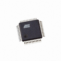
ATMEGA406-1AAU Atmel, ATMEGA406-1AAU Datasheet - Page 109

ATMEGA406-1AAU
Manufacturer Part Number
ATMEGA406-1AAU
Description
IC AVR MCU 40K 1MHZ 48LQFP
Manufacturer
Atmel
Series
AVR® ATmegar
Specifications of ATMEGA406-1AAU
Core Processor
AVR
Core Size
8-Bit
Speed
1MHz
Connectivity
I²C
Peripherals
POR, WDT
Number Of I /o
18
Program Memory Size
40KB (20K x 16)
Program Memory Type
FLASH
Eeprom Size
512 x 8
Ram Size
2K x 8
Voltage - Supply (vcc/vdd)
4 V ~ 25 V
Data Converters
A/D 10x12b
Oscillator Type
Internal
Operating Temperature
-30°C ~ 85°C
Package / Case
48-LQFP
Processor Series
ATMEGA48x
Core
AVR8
Data Bus Width
8 bit
Data Ram Size
2 KB
Interface Type
2-Wire
Maximum Clock Frequency
1 MHz
Number Of Programmable I/os
18
Number Of Timers
2
Maximum Operating Temperature
+ 85 C
Mounting Style
SMD/SMT
3rd Party Development Tools
EWAVR, EWAVR-BL
Development Tools By Supplier
ATAVRDRAGON, ATSTK500, ATSTK600, ATAVRISP2, ATAVRONEKIT
Minimum Operating Temperature
- 30 C
Cpu Family
ATmega
Device Core
AVR
Device Core Size
8b
Frequency (max)
1MHz
Total Internal Ram Size
2KB
# I/os (max)
18
Number Of Timers - General Purpose
2
Operating Supply Voltage (typ)
5/9/12/15/18/24V
Operating Supply Voltage (max)
25V
Operating Supply Voltage (min)
4V
On-chip Adc
10-chx12-bit
Instruction Set Architecture
RISC
Operating Temp Range
-30C to 85C
Operating Temperature Classification
Commercial
Mounting
Surface Mount
Pin Count
48
Package Type
LQFP
Controller Family/series
AVR MEGA
No. Of I/o's
18
Eeprom Memory Size
512Byte
Ram Memory Size
2KB
Cpu Speed
1MHz
Rohs Compliant
Yes
For Use With
770-1007 - ISP 4PORT ATMEL AVR MCU SPI/JTAG770-1005 - ISP 4PORT FOR ATMEL AVR MCU JTAG770-1004 - ISP 4PORT FOR ATMEL AVR MCU SPI
Lead Free Status / RoHS Status
Lead free / RoHS Compliant
Available stocks
Company
Part Number
Manufacturer
Quantity
Price
Part Number:
ATMEGA406-1AAU
Manufacturer:
AT
Quantity:
20 000
- Current page: 109 of 263
- Download datasheet (3Mb)
18.2.1
2548E–AVR–07/06
CADCSRA – CC-ADC Control and Status Register A
charge flow estimation should be based on the self-discharge rate of the battery and the standby
current of the battery system.
• Bit 7 – CADEN: CC-ADC Enable
When the CADEN bit is cleared (zero), the CC-ADC is disabled, and any ongoing conversions
will be terminated. When the CADEN bit is set (one), the CC-ADC will continuously measure the
voltage drop over the external sense resistor R
abled. Note that the bandgap voltage reference must be enabled separately, see
Bandgap Calibration C Register” on page
• Bit 6 – Res: Reserved
This bit is reserved bit in the ATmega406 and will always read as zero.
• Bit 5 - CADUB: CC-ADC Update Busy
The CC-ADC operates in a different clock domain than the CPU. Whenever a new value is writ-
ten to CADCSRA, CADRCC or CADRDC, this value must be synchronized to the CC-ADC clock
domain. Subsequent writes to these registers will be blocked during this synchronization. Syn-
chronization of one of the registers, will block updating of all the others. The CADUB bit will be
read as one while any of these registers is being synchronized, and will be read as zero when
neither register is being synchronized.
• Bits 4:3 – CADAS1:0: CC-ADC Accumulate Current Select
The CADAS bits select the conversion time for the Accumulate Current output as shown in
18-1.
Table 18-1.
Bit
(0xE4)
Read/Write
Initial Value
CADAS1:0
00
01
10
11
CADEN
CC-ADC Accumulate Current Conversion Time
R/W
7
0
R
6
0
–
CADUB
R
5
0
CC-ADC Accumulate Current Conversion Time
CADAS1
R/W
123.
4
0
SENSE
CADAS0
R/W
3
0
. In Power-off, the CC-ADC is always dis-
125 ms
250 ms
500 ms
CADSI1
1 s
R/W
2
0
CADSI0
R/W
1
0
ATmega406
CADSE
R/W
0
0
”BGCCR –
CADCSRA
Table
109
Related parts for ATMEGA406-1AAU
Image
Part Number
Description
Manufacturer
Datasheet
Request
R

Part Number:
Description:
Manufacturer:
Atmel Corporation
Datasheet:

Part Number:
Description:
IC AVR MCU 2.4GHZ XCEIVER 64QFN
Manufacturer:
Atmel
Datasheet:

Part Number:
Description:
Manufacturer:
Atmel
Datasheet:

Part Number:
Description:
MCU ATMEGA644/AT86RF230 40-DIP
Manufacturer:
Atmel
Datasheet:

Part Number:
Description:
BUNDLE ATMEGA644P/AT86RF230 QFN
Manufacturer:
Atmel
Datasheet:

Part Number:
Description:
BUNDLE ATMEGA644P/AT86RF230 TQFP
Manufacturer:
Atmel
Datasheet:

Part Number:
Description:
MCU ATMEGA1281/AT86RF230 64-TQFP
Manufacturer:
Atmel
Datasheet:

Part Number:
Description:
MCU ATMEGA1280/AT86RF230 100TQFP
Manufacturer:
Atmel
Datasheet:

Part Number:
Description:
BUNDLE ATMEGA1280/AT86RF100-TQFP
Manufacturer:
Atmel
Datasheet:

Part Number:
Description:
BUNDLE ATMEGA2560V/AT86RF230-ZU
Manufacturer:
Atmel
Datasheet:

Part Number:
Description:
MCU ATMEGA2561/AT86RF230 64-TQFP
Manufacturer:
Atmel
Datasheet:

Part Number:
Description:
MCU ATMEGA2560/AT86RF230 100TQFP
Manufacturer:
Atmel
Datasheet:

Part Number:
Description:
MCU ATMEGA2561/AT86RF230 64-QFN
Manufacturer:
Atmel
Datasheet:

Part Number:
Description:
MCU, 8BIT, AVR, 16K FLASH, 28PDIP
Manufacturer:
Atmel
Datasheet:

Part Number:
Description:
Microcontroller Modules MCU CARD BIGAVR6 100P W/ ATMEGA2560
Manufacturer:
mikroElektronika


