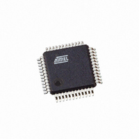
ATMEGA406-1AAU Atmel, ATMEGA406-1AAU Datasheet - Page 37

ATMEGA406-1AAU
Manufacturer Part Number
ATMEGA406-1AAU
Description
IC AVR MCU 40K 1MHZ 48LQFP
Manufacturer
Atmel
Series
AVR® ATmegar
Specifications of ATMEGA406-1AAU
Core Processor
AVR
Core Size
8-Bit
Speed
1MHz
Connectivity
I²C
Peripherals
POR, WDT
Number Of I /o
18
Program Memory Size
40KB (20K x 16)
Program Memory Type
FLASH
Eeprom Size
512 x 8
Ram Size
2K x 8
Voltage - Supply (vcc/vdd)
4 V ~ 25 V
Data Converters
A/D 10x12b
Oscillator Type
Internal
Operating Temperature
-30°C ~ 85°C
Package / Case
48-LQFP
Processor Series
ATMEGA48x
Core
AVR8
Data Bus Width
8 bit
Data Ram Size
2 KB
Interface Type
2-Wire
Maximum Clock Frequency
1 MHz
Number Of Programmable I/os
18
Number Of Timers
2
Maximum Operating Temperature
+ 85 C
Mounting Style
SMD/SMT
3rd Party Development Tools
EWAVR, EWAVR-BL
Development Tools By Supplier
ATAVRDRAGON, ATSTK500, ATSTK600, ATAVRISP2, ATAVRONEKIT
Minimum Operating Temperature
- 30 C
Cpu Family
ATmega
Device Core
AVR
Device Core Size
8b
Frequency (max)
1MHz
Total Internal Ram Size
2KB
# I/os (max)
18
Number Of Timers - General Purpose
2
Operating Supply Voltage (typ)
5/9/12/15/18/24V
Operating Supply Voltage (max)
25V
Operating Supply Voltage (min)
4V
On-chip Adc
10-chx12-bit
Instruction Set Architecture
RISC
Operating Temp Range
-30C to 85C
Operating Temperature Classification
Commercial
Mounting
Surface Mount
Pin Count
48
Package Type
LQFP
Controller Family/series
AVR MEGA
No. Of I/o's
18
Eeprom Memory Size
512Byte
Ram Memory Size
2KB
Cpu Speed
1MHz
Rohs Compliant
Yes
For Use With
770-1007 - ISP 4PORT ATMEL AVR MCU SPI/JTAG770-1005 - ISP 4PORT FOR ATMEL AVR MCU JTAG770-1004 - ISP 4PORT FOR ATMEL AVR MCU SPI
Lead Free Status / RoHS Status
Lead free / RoHS Compliant
Available stocks
Company
Part Number
Manufacturer
Quantity
Price
Part Number:
ATMEGA406-1AAU
Manufacturer:
AT
Quantity:
20 000
8.7
8.7.1
8.7.2
8.7.3
8.7.4
8.7.5
2548E–AVR–07/06
Minimizing Power Consumption
Watchdog Timer
Port Pins
On-chip Debug System
Battery Protection
Voltage ADC
There are several issues to consider when trying to minimize the power consumption in an AVR
controlled system. In general, sleep modes should be used as much as possible, and the sleep
mode should be selected so that as few as possible of the device’s functions are operating. All
functions not needed should be disabled. In particular, the following modules may need special
consideration when trying to achieve the lowest possible power consumption.
If the Watchdog Timer is not needed in the application, the module should be turned off. If the
Watchdog Timer is enabled, it will be enabled in all sleep modes except Power-off. The Watch-
dog Timer current consumption is significant only in Power-down mode. See
on page 43
When entering a sleep mode, all port pins should be configured to use minimum power. The
most important is then to ensure that no pins drive resistive loads. In sleep modes where both
the I/O clock (clk
be disabled. This ensures that no power is consumed by the input logic when not needed. In
some cases, the input logic is needed for detecting wake-up conditions, and it will then be
enabled. See
enabled. If the input buffer is enabled and the input signal is left floating or have an analog signal
level close to V
For analog input pins, the digital input buffer should be disabled at all times. An analog signal
level close to V
input buffers can be disabled by writing to the Digital Input Disable Register. Refer to
Digital Input Disable Register 0” on page 120
If the On-chip debug system is enabled by OCDEN Fuse and the chip enters sleep mode, the
main clock source is enabled, and hence, always consumes power. In the deeper sleep modes,
this will contribute significantly to the total current consumption.
If one of the Battery Protection features is not needed by the application, this feature should be
disabled, see
FET is switched off, the Short-Circuit Circuitry will automatically be stopped in order to minimize
power consumption. The current consumption in the Battery Protection circuitry is only signifi-
cant in Power-down mode.
If enabled, the V-ADC will consume power independent of sleep mode. To save power, the V-
ADC should be disabled when not used, and before entering Power-save or Power-down sleep
modes. See
116
for details on V-ADC operation.
for details on how to configure the Watchdog Timer.
”Voltage ADC – 10-channel General Purpose 12-bit Sigma-Delta ADC” on page
”Digital Input Enable and Sleep Modes” on page 64
”BPCR – Battery Protection Control Register” on page
REG
REG
I/O
/2, the input buffer will use excessive power.
) and the ADC clock (clk
/2 on an input pin can cause significant current even in active mode. Digital
ADC
for details.
) are stopped, the input buffers of the device will
for details on which pins are
128. When the Discharge
ATmega406
”Watchdog Timer”
”DIDR0 –
37


