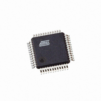
ATMEGA406-1AAU Atmel, ATMEGA406-1AAU Datasheet - Page 149

ATMEGA406-1AAU
Manufacturer Part Number
ATMEGA406-1AAU
Description
IC AVR MCU 40K 1MHZ 48LQFP
Manufacturer
Atmel
Series
AVR® ATmegar
Specifications of ATMEGA406-1AAU
Core Processor
AVR
Core Size
8-Bit
Speed
1MHz
Connectivity
I²C
Peripherals
POR, WDT
Number Of I /o
18
Program Memory Size
40KB (20K x 16)
Program Memory Type
FLASH
Eeprom Size
512 x 8
Ram Size
2K x 8
Voltage - Supply (vcc/vdd)
4 V ~ 25 V
Data Converters
A/D 10x12b
Oscillator Type
Internal
Operating Temperature
-30°C ~ 85°C
Package / Case
48-LQFP
Processor Series
ATMEGA48x
Core
AVR8
Data Bus Width
8 bit
Data Ram Size
2 KB
Interface Type
2-Wire
Maximum Clock Frequency
1 MHz
Number Of Programmable I/os
18
Number Of Timers
2
Maximum Operating Temperature
+ 85 C
Mounting Style
SMD/SMT
3rd Party Development Tools
EWAVR, EWAVR-BL
Development Tools By Supplier
ATAVRDRAGON, ATSTK500, ATSTK600, ATAVRISP2, ATAVRONEKIT
Minimum Operating Temperature
- 30 C
Cpu Family
ATmega
Device Core
AVR
Device Core Size
8b
Frequency (max)
1MHz
Total Internal Ram Size
2KB
# I/os (max)
18
Number Of Timers - General Purpose
2
Operating Supply Voltage (typ)
5/9/12/15/18/24V
Operating Supply Voltage (max)
25V
Operating Supply Voltage (min)
4V
On-chip Adc
10-chx12-bit
Instruction Set Architecture
RISC
Operating Temp Range
-30C to 85C
Operating Temperature Classification
Commercial
Mounting
Surface Mount
Pin Count
48
Package Type
LQFP
Controller Family/series
AVR MEGA
No. Of I/o's
18
Eeprom Memory Size
512Byte
Ram Memory Size
2KB
Cpu Speed
1MHz
Rohs Compliant
Yes
For Use With
770-1007 - ISP 4PORT ATMEL AVR MCU SPI/JTAG770-1005 - ISP 4PORT FOR ATMEL AVR MCU JTAG770-1004 - ISP 4PORT FOR ATMEL AVR MCU SPI
Lead Free Status / RoHS Status
Lead free / RoHS Compliant
Available stocks
Company
Part Number
Manufacturer
Quantity
Price
Part Number:
ATMEGA406-1AAU
Manufacturer:
AT
Quantity:
20 000
25.6.4
25.6.5
2548E–AVR–07/06
TWDR – TWI Data Register
TWAR – TWI (Slave) Address Register
Table 25-2.
To calculate bit rates, see
in the equation.
In Transmit mode, TWDR contains the next byte to be transmitted. In Receive mode, the TWDR
contains the last byte received. It is writable while the TWI is not in the process of shifting a byte.
This occurs when the TWI Interrupt Flag (TWINT) is set by hardware. Note that the data register
cannot be initialized by the user before the first interrupt occurs. The data in TWDR remains sta-
ble as long as TWINT is set. While data is shifted out, data on the bus is simultaneously shifted
in. TWDR always contains the last byte present on the bus, except after a wake-up from a sleep
mode by the TWI interrupt. In this case, the contents of TWDR is undefined. In the case of a lost
bus arbitration, no data is lost in the transition from Master to Slave. Handling of the ACK bit is
controlled automatically by the TWI logic, the CPU cannot access the ACK bit directly.
• Bits 7:0 – TWD: TWI Data Register
These eight bits constitute the next data byte to be transmitted, or the latest data byte received
on the Two-wire Serial Bus.
The TWAR should be loaded with the 7-bit slave address (in the seven most significant bits of
TWAR) to which the TWI will respond when programmed as a slave transmitter or Receiver, and
not needed in the Master modes. In multi-master systems, TWAR must be set in masters which
can be addressed as slaves by other masters.
The LSB of TWAR is used to enable recognition of the general call address (0x00). There is an
associated address comparator that looks for the slave address (or general call address if
enabled) in the received serial address. If a match is found, an interrupt request is generated.
• Bits 7:1 – TWA: TWI (Slave) Address Register
These seven bits constitute the slave address of the TWI unit.
Bit
(0xBB)
Read/Write
Initial Value
Bit
(0xBA)
Read/Write
Initial Value
TWPS1
0
0
1
1
TWI Bit Rate Prescaler
TWD7
TWA6
R/W
R/W
7
1
7
1
TWD6
TWA5
R/W
R/W
”Bit Rate Generator Unit” on page
6
1
6
1
TWD5
TWA4
TWPS0
R/W
R/W
5
1
5
1
0
1
0
1
TWD4
TWA3
R/W
R/W
4
1
4
1
TWA2
TWD3
R/W
R/W
1
3
1
3
145. The value of TWPS1:0 is used
TWA1
TWD2
R/W
R/W
2
1
2
1
Prescaler Value
TWA0
TWD1
R/W
R/W
1
1
1
1
16
64
1
4
ATmega406
TWGCE
TWD0
R/W
R/W
0
1
0
0
TWDR
TWAR
149


